
materials
Article
Spectroscopic Analysis of Rare-Earth Silicide Structures on the
Si(111) Surface
Simone Sanna 1,* , Julian Plaickner 2, Kris Holtgrewe 1, Vincent M. Wettig 1, Eugen Speiser 3,
Sandhya Chandola 2and Norbert Esser 3,4
Citation: Sanna, S.; Plaickner, J.;
Holtgrewe, K.; Wettig, V.M.;
Speiser, E.; Chandola, S.; Esser, N.
Spectroscopic Analysis of Rare-Earth
Silicide Structures on the Si(111)
Surface. Materials 2021,14, 4104.
https://doi.org/10.3390/ma
14154104
Academic Editor: Mariusz Krawiec
Received: 24 June 2021
Accepted: 20 July 2021
Published: 23 July 2021
Publisher’s Note: MDPI stays neutral
with regard to jurisdictional claims in
published maps and institutional affil-
iations.
Copyright: © 2021 by the authors.
Licensee MDPI, Basel, Switzerland.
This article is an open access article
distributed under the terms and
conditions of the Creative Commons
Attribution (CC BY) license (https://
creativecommons.org/licenses/by/
4.0/).
1
Institut für Theoretische Physik and Center for Materials Research (LaMa), Justus-Liebig-Universität Gießen,
Vincent.M.W[email protected] (V.M.W.)
2
Helmholtz-Zentrum Berlin für Materialen und Energie GmbH, Hahn-Meitner Platz 1, 14109 Berlin, Germany;
3Leibniz-Institut für Analytische Wissenschaften-ISAS-e.V., Schwarzschildstr. 8, 12489 Berlin, Germany;
4Institut für Festkörperphysik, Technische Universität Berlin, Hardenbergstr. 36, 10623 Berlin, Germany
*Correspondence: [email protected]; Tel.: +49-641-99-33362
Abstract:
Two-dimensional rare-earth silicide layers deposited on silicon substrates have been
intensively investigated in the last decade, as they can be exploited both as Ohmic contacts or as
photodetectors, depending on the substrate doping. In this study, we characterize rare-earth silicide
layers on the Si(111) surface by a spectroscopic analysis. In detail, we combine Raman and reflectance
anisotropy spectroscopy (RAS) with first-principles calculations in the framework of the density
functional theory. RAS suggests a weakly isotropic surface, and Raman spectroscopy reveals the
presence of surface localized phonons. Atomistic calculations allow to assign the detected Raman
peaks to phonon modes localized at the silicide layer. The good agreement between the calculations
and the measurements provides a strong argument for the employed structural model.
Keywords:
surface science; Si(111); rare earth silicide; terbium silicide; Raman spectroscopy; RAS;
density functional theory; DFT; thin films; 2D material
1. Introduction
Rare earth (RE) deposition on Si substrates followed by thermal annealing leads to the
formation of various structures consisting of rare-earth silicides of different composition.
The amount of deposited rare earths, the substrate orientation, and the annealing process
can be exploited to obtain structures of different dimensionality (from one dimensional
(1D) to three-dimensional (3D)), periodicity, and morphology.
Quasi-1D metallic nanowires of different rare-earth silicides [
1
–
6
] grow on Si(001)
substrates and vicinal surfaces [
7
–
15
]. Due to their highly anisotropic growth, the wires are
interesting model systems for the realization of 1D physics [
16
–
20
] or as building blocks
for nanoelectronics applications [21–25].
The 2D films of rare-earth silicides can be epitaxially grown on the Si(111). Most
trivalent rare-earth elements lead to surface reconstructions of related morphology and
electronic properties [
26
–
34
]. The silicide layers have been exploited both as Ohmic contacts
(due to the low Schottky-barrier heights) on
n
-type Si substrates or as photodetectors on
p-type Si substrates [35,36].
Among the known rare-earth induced reconstructions of the Si(111) surface, a metallic
phase consisting of a regular, stoichiometric RESi
2
silicide monolayer (ML) of (1
×
1)
periodicity, and a further metallic phase consisting of a regular RE
3
Si
5
silicide bilayer of
(√3×√3) periodicity are the most intensively investigated structures.
Although different experimental studies have been dedicated to the characterization
of the silicide layers, their lattice dynamics is completely unknown. In this manuscript,
Materials 2021,14, 4104. https://doi.org/10.3390/ma14154104 https://www.mdpi.com/journal/materials

Materials 2021,14, 4104 2 of 18
we investigate experimentally (on the example of terbium silicide) and theoretically (for
all lanthanides) the vibrational properties of silicide layers of different height. Surface-
localized phonon modes can be observed at the terbium silicide surface layer, which do not
substantially depend on the system temperature. Moreover, optical absorption features are
identified in reflectance anisotropy spectroscopy (RAS), which can be related to interband
transitions within the Tb-Si surface electronic band structure.
Corresponding atomistic calculations allow to assign the detected Raman peaks to
phonon modes in the (1
×
1)-periodic monolayer structure, which are localized in the
silicide. A roughly linear dependence of the Raman shifts on the atomic number of the
considered rare earth is predicted, which correlates with the bond lengths of the different
silicides. Structure specific phonon modes are found for the silicide monolayer of (1
×
1)
periodicity and for the silicide bilayer of (
√3×√3
) periodicity, which, in principle, allow
for a structural determination on the basis of the Raman spectra.
The good agreement between the calculations and the measurements strongly sup-
ports the employed structural model.
2. Materials and Methods
2.1. Sample Preparation
Vicinal Si(111) substrates with a miscut angle of 4
±
1
◦
degree were cut from com-
mercial
n
-type Si(111) wafers and cleaned in an ultra-high vacuum (UHV) by degassing
for 12 h at 600
◦
C. Then, repeated flash annealing up to 1200
◦
C was applied followed by
slow cooling down from 850
◦
C at a rate of about 1
◦
C/s to obtain a well-ordered clean
(7
×
7) surface. Spot splitting of the integer spots were observed by low energy electron
diffraction (LEED, not shown) due to the presence of steps resulting from the miscut angle.
Annealing temperatures were measured by an infrared pyrometer. The Tb silicide struc-
tures were grown in situ by depositing Tb onto the clean Si(111)-(7
×
7) surface held at
room temperature followed by annealing at 520
◦
C for 2 min to form the silicide structures.
In this work, the Tb coverage is given in monolayers (ML), with 1ML corresponding to
the surface atom density at the unreconstructed Si(111) surface (7.8
×
10
14
atoms/cm
2
).
The base pressure was better than 1
×
10
−10
mbar and did not exceed 5
×
10
−10
mbar
during preparation, ruling out any form of contamination. The deposited Tb amount was
determined by identifying the parameters for the different growth regimes, namely the
submonolayer, monolayer, and multilayer regimes known from previous publications [
28
].
For submonolayer Tb coverages (about 0.4ML Tb annealed at 550
◦
C), a (2
√3×
2
√3
)
R30
◦
superstructure is observed with LEED, in agreement with available data [
28
]. In the
monolayer regime, (about 1ML Tb, annealed at 550
◦
C) the TbSi
2
monolayer with (1
×
1)
periodicity described in the following sections is formed, while a strong (
√3×√3
) R30
◦
LEED pattern is observed for the multilayer regime (coverage exceeding 1ML Tb), which
is again in agreement with the literature [
28
]. We remark that between the monolayer and
multilayer regime, Tb silicide islands of different morphology and periodicity start to grow,
which coalesce to form closed layers after thermal treatment. These structures correspond
either to the two-dimensional hexagonal TbSi
2
monolayer with (1
×
1) periodicity or to the
higher hexagonal Tb
3
Si
5
multilayer structures with (
√3×√3
) periodicity, which are also
described in the following. This regime is called the monolayer-to-multilayer regime [28].
In our experimental investigation, we employ Tb as a representative trivalent rare-
earth. Tb silicide phases belong to the group of silicide structures of the trivalent rare-earth
metals, which have very similar structural, chemical, and electronic properties [
26
]. They
are described by the same structural models, based on the defect-free, hexagonal rare-earth
disilicides. This notwithstanding, slightly differing procedures might be necessary to
crystallize silicides of different rare earths. Although the growth of Tb on Si(111) displays
very similar characteristics as observed for other trivalent rare-earth metals such as Gd, Dy,
or Er, which all feature the previously described growth regimes [
28
,
37
,
38
], some of the light
rare earths might present peculiarities in their growth process. The discussion of the growth
process of the different lanthanides is beyond the scope of this investigation, though.
Materials 2021,14, 4104 3 of 18
2.2. Experimental Setup
Raman measurements were obtained using a Dilor triple spectrometer and a Si-based
high-efficiency CCD detector. The excitation wavelength of 458nm (2.70eV photon energy)
was generated by an Ar
+
ion laser operated at a power of approximately 400mW. The
Raman spectra were calibrated using 9 different Ar
+
laser plasma lines. The spectral
resolution was obtained from the Gauss width of the plasma lines, and is equal to 3.5cm
−1
.
The measured Raman spectra contain bulk and surface contributions that were separated
from each other according to the procedure described in Appendix A.
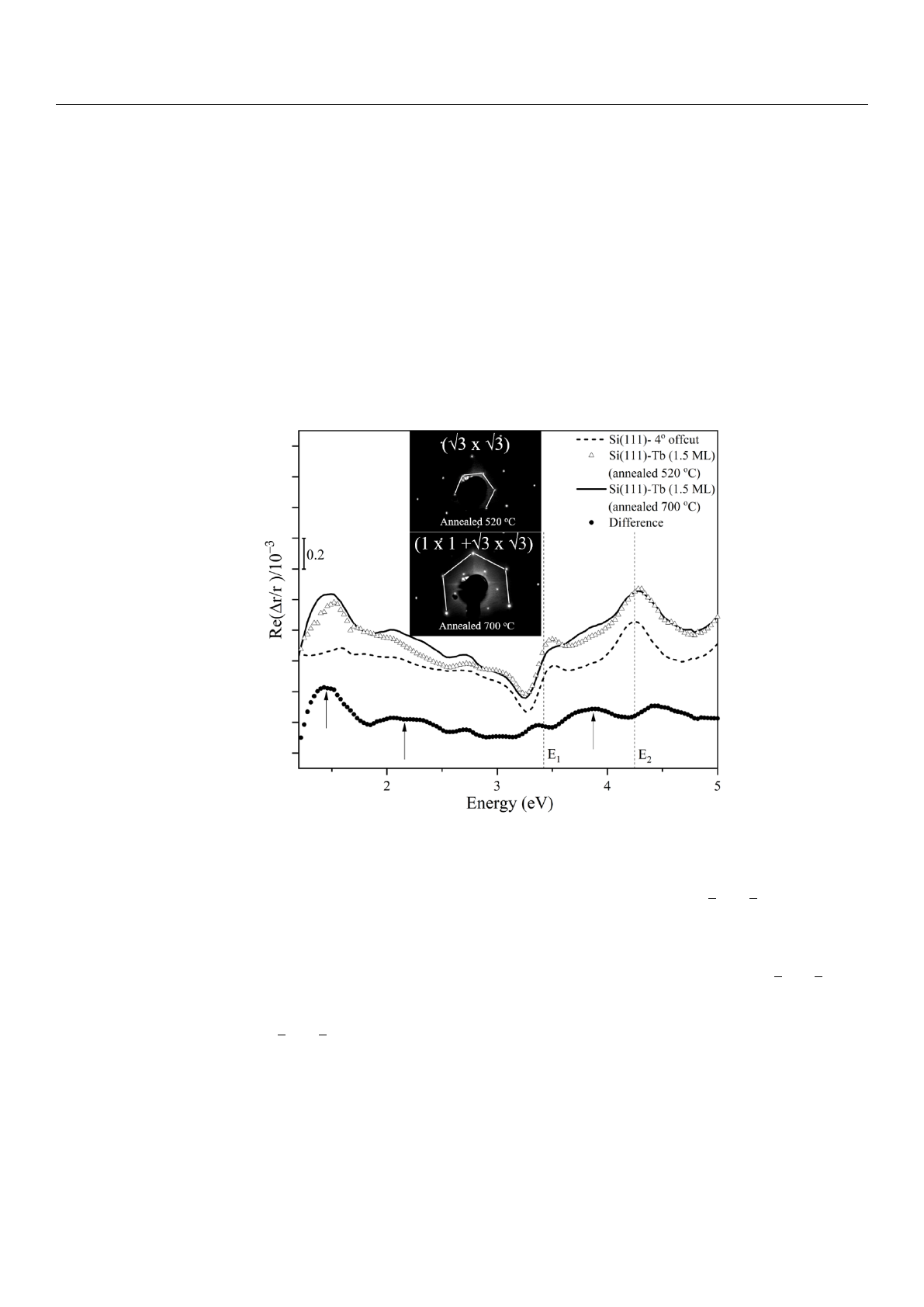
Figure 1shows a RAS spectrum obtained with 1.5ML Tb on the Si(111) substrate.
The arrows indicate relevant optical transitions at 1.4, 2.2, and 3.8eV. According to the
electronic band structure published in previous works [
8
,
26
], the optical absorption seems
to be related to electronic transitions within the surface electronic band structure, which
becomes anisotropic due to presence of the step edges on the vicinal Si substrate.
Figure 1.
Reflectance anisotropy spectrum obtained before and after deposition of 1.5ML Tb on the
4
◦
-offcut Si(111) substrate and annealing at different temperatures. The upper (lower) inset shows
the corresponding LEED pattern after annealing at 520◦C (700 ◦C).
The LEED pattern in the upper inset of Figure 1shows a (
√3×√3
) reconstruction.
However, no modes at all were detected in Raman measurements for this surface. Raman
signatures could be only detected after a further annealing at a higher temperature of
700
◦
C. The LEED analysis (lower inset of Figure 1) showed that the bulk (1
×
1) spots
became much stronger than those of the surface annealed at 520
◦
C. The (
√3×√3
) spots
are still visible, though less sharp and with a much higher background. This indicates
the formation of a broad, surface-covering (1
×
1) monolayer, which contains smaller
(
√3×√3
) islands. This is in agreement with the previously mentioned coalescence of
silicide islands into homogeneous layers in the monolayer-to-multilayer regime [28].
We would like to note that the surface Raman spectra, as shown in Figure 2or
Figure A2
in Appendix A, are always reproducible after the annealing at 700
◦
C, while at
lower annealing temperatures no surface modes are visible at all. This may be related to
the complex stoichiometry of the Tb/Si surface, which consists of a mix of different phases
after annealing at low temperatures, and develops into a larger fraction of (1
×
1) islands
only after the high-temperature annealing [
28
,
39
]. Moreover, the surface morphology may
contribute to an enhancement of the surface Raman signal, for instance due to momentum
Materials 2021,14, 4104 4 of 18
conservation relaxation or by local field enhancement effects. Finally, we note that the
surface Raman signal was sensitively dependent on small contamination by residual gas,
since the surface Raman signal of fresh preparations diminished rapidly within a few hours
in UHV. This supports the surface origin of the recorded Raman signal.
2.3. Computational Details
The spectroscopic signatures of the TbSi
2
monolayer on the Si(111) surface are modeled
within density functional theory (DFT). The calculations are performed in the framework
of the generalized gradient approximation [
40
] (GGA) in the PBEsol formulation [
41
,
42
] as
implemented in the Vienna ab initio simulation package (VASP) [43,44].
Projector augmented wave [
45
,
46
] (PAW) potentials with projectors up to
l=
1 for H,
l=
2 for Si and
l=
3 for Tb and the other rare earths have been used. As no other valence
state than RE
3+
has been observed for Tb ions in the silicide structures, we constrain the Tb
valence state treating
n−
1
f
-electrons as core states. This approach, commonly referred to
as frozen-core method, allows for a proper treatment of the lanthanides within DFT [
47
–
49
].
We have verified in a previous work [
1
] that keeping the
f
electrons frozen in the atomic
core plays a negligible role in the structural properties of stochiometric bulk hexagonal rare
earth silicides, leading only to variations in the lattice parameters smaller than 0.01Å.
To ensure numerical convergence, the electronic wave functions are expanded into
plane waves up to an energy cutoff of 400eV, while the Brillouin zone is sampled by a
20
×
20
×
1
Γ
-centered Monkhorst-Pack mesh [
50
] in the case of the monolayer structure
with (1
×
1) periodicity and by a 12
×
12
×
1
Γ
-centered mesh in the case of the bilayer
structure with (√3×√3) periodicity.
Planar TbSi
2
silicide layers on the Si(111) are modeled with slabs consisting of 10 Si
layers stacked along the (111) crystallographic direction (modeling the substrate), the
silicide monolayer, and a vacuum region of at least 20Å. The dangling bonds at the
bottom face of the slabs are saturated by hydrogen atoms. Structural optimization is
performed until the residual Hellmann–Feynman forces [
51
] are lower than 0.001 eV/Å. In
this procedure, the silicide layer and 6 Si bilayers are free to relax, while 4 Si layers and the
hydrogen atoms are kept fixed at the bulk positions in order to model the substrate.
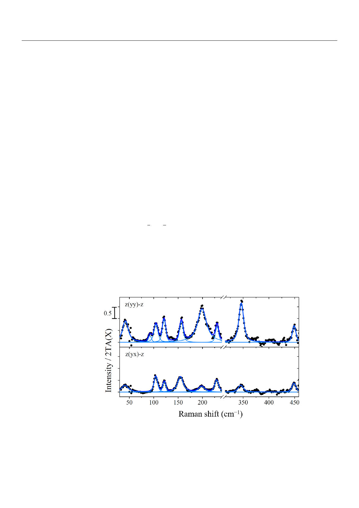
Figure 2.
Surface Raman spectra of the terbium silicide layer grown on 4
◦
-offcut Si(111) substrate
for parallel z(yy)-z and crossed z(yx)-z polarization configurations. The spectra are fitted with Voigt
profiles with a fixed Gauss width equal to the spectral resolution of 3.5cm−1.

Materials 2021,14, 4104 5 of 18
3. Results
3.1. Vibrational Modes of the Tb-Layer on 4◦-Offcut Si(111)
Figure 2shows the surface Raman spectra of the terbium silicide layer on 4
◦
-offcut
Si(111) substrates for different polarization configurations. The spectra are fitted with Voigt
profiles with a fixed Gauss width equal to the spectral resolution of 3.5cm
−1
. Measured
Raman frequencies and mode symmetry according to polarization selection rules are
indicated in Table 1.
Table 1.
Measured Raman frequencies (in cm
−1
) of the Tb-reconstruction grown on 4
◦
-offcut Si(111)
substrate.
4◦-Offcut z(yy)-z 4◦-Offcut z(yx)-z Symm.
41.5 ±1.2 41.5 ±1.3 A
92.0 ±2A
104.3 ±1.1 103.9 ±0.7 E
121.0 ±0.7 121.9 ±0.6 E
156.8 ±1.2 154.6 ±1.2 E
198.8 ±0.8 197.9 ±1.4 A
229.8 ±0.9 229.0 ±0.7 A
346.4 ±0.8 345.5 ±1.3 A
449.1 ±1.2 448.7 ±1.1 A
Within the threefold symmetry of the ideal hexagonal Si(111) surface, phonon modes
of
A
and
E
symmetry are expected. Due to the Raman selection rules,
A
modes are
observable in parallel polarization (the symmetry equivalent
xx
or
yy
configurations),
while
E
modes are detectable within crossed polarization (the symmetry equivalent
xy
and
yx
configurations). Due to the symmetry reduction by atomic steps (4
◦
offcut) and
the possibly inhomogeneous surface morphology, the symmetry properties are not strictly
mirrored in Raman experiments, but according changes in scattering intensity are still
observable. Indeed, the Raman spectra measured in crossed and parallel polarization
configuration show some differences. The bands at 41.5cm
−1
, 198.8cm
−1
and 346.4cm
−1
exhibit much higher intensity in parallel polarization, while the bands at 104.3cm
−1
and
156.8cm−1are of comparable intensity in both scattering configurations.
On the basis of the relative Raman intensity measured in parallel and crossed po-
larization, we tentatively assign the mode symmetry as shown in the third column of
Table 1
. The close agreement of spectra recorded in
xx
and
yy
configuration, as well as in
xy
and
yx
configuration (shown in Figure A2 in the Appendix A), demonstrates the high
reproducibility of the difference spectra we employ to characterize the silicide layers.
The Raman modes observed in the surface spectrum overlap, at least partially, with
the bulk phonon branches of Si. As shown previously on different Si(
hhk
)-Au systems,
surfaces resonances may arise by coupling to bulk phonon modes close to the Brillouin
zone boundaries, activated by the surface modification [
52
]. Therefore, part of the observed
modes will have predominant bulk character, while others will be mostly surface localized.
This issue will be addressed in detail by the ab initio calculations described in the following.
To discriminate whether the measured Raman signatures are related to true surface
localized phonon modes or rather to surface-activated bulk resonances, we compare them
with the phonon dispersion of bulk Si, which we have calculated within DFT-PBEsol.
Figure 3shows the calculated dispersion and the corresponding density of states (DOS), in
which we overlay the measured Raman signatures as horizontal dashed lines.
Loading more pages...