Appl. Phys. Lett. 116, 121101 (2020); https://doi.org/10.1063/1.5143297 116, 121101
© 2020 Author(s).
Thin-film flip-chip UVB LEDs realized by
electrochemical etching
Cite as: Appl. Phys. Lett. 116, 121101 (2020); https://doi.org/10.1063/1.5143297
Submitted: 21 December 2019 . Accepted: 11 March 2020 . Published Online: 24 March 2020
Michael A. Bergmann , Johannes Enslin , Filip Hjort , Tim Wernicke , Michael Kneissl , and Åsa
Haglund
COLLECTIONS
This paper was selected as an Editor’s Pick
ARTICLES YOU MAY BE INTERESTED IN
On-wafer fabrication of etched-mirror UV-C laser diodes with the ALD-deposited DBR
Applied Physics Letters 116, 122101 (2020); https://doi.org/10.1063/1.5145017
Modulation of the two-dimensional electron gas channel in flexible AlGaN/GaN high-electron-
mobility transistors by mechanical bending
Applied Physics Letters 116, 123501 (2020); https://doi.org/10.1063/1.5142546
A perspective on blue TADF materials based on carbazole-benzonitrile derivatives for efficient
and stable OLEDs
Applied Physics Letters 116, 120503 (2020); https://doi.org/10.1063/1.5143501

Thin-film flip-chip UVB LEDs realized by
electrochemical etching
Cite as: Appl. Phys. Lett. 116, 121101 (2020); doi: 10.1063/1.5143297
Submitted: 21 December 2019 .Accepted: 11 March 2020 .
Published Online: 24 March 2020
Michael A. Bergmann,
1,a)
Johannes Enslin,
2
Filip Hjort,
1
Tim Wernicke,
2
Michael Kneissl,
2
and A
˚sa Haglund
1
AFFILIATIONS
1
Department of Microtechnology and Nanoscience, Chalmers University of Technology, 41296 Gothenburg, Sweden
2
Institute of Solid State Physics, Technische Universit€
at Berlin, 10623 Berlin, Germany
a)
Author to whom correspondence should be addressed: michael.bergmann@chalmers.se
ABSTRACT
We demonstrate a thin-film flip-chip (TFFC) light-emitting diode (LED) emitting in the ultraviolet B (UVB) at 311 nm, where substrate
removal has been achieved by electrochemical etching of a sacrificial Al0:37Ga0:63N layer. The electroluminescence spectrum of the TFFC
LED corresponds well to the as-grown LED structure, showing no sign of degradation of structural and optical properties by electrochemical
etching. This is achieved by a proper epitaxial design of the sacrificial layer and the etch stop layers in relation to the LED structure and the
electrochemical etch conditions. Enabling a TFFC UV LED is an important step toward improving the light extraction efficiency that limits
the power conversion efficiency in AlGaN-based LEDs.
V
C2020 Author(s). All article content, except where otherwise noted, is licensed under a Creative Commons Attribution (CC BY) license (http://
creativecommons.org/licenses/by/4.0/).https://doi.org/10.1063/1.5143297
Ultraviolet (UV) light sources are used in a number of applica-
tions such as water disinfection, UV curing, and phototherapy.
1
UV
light-emitting diodes (LEDs) are expected to replace conventional UV
light sources like mercury gas discharge lamps due to their small form
factor, robustness, environmentally friendly materials, and selectable
emission wavelength.
2
However, the poor power conversion efficiency
of UV LEDs below 10% for wavelengths shorter than 350 nm, see Ref.
2, strongly limits their widespread use.
One of the major factors limiting the power conversion efficiency
is the light extraction efficiency (LEE),
2
which can be improved by a
thin-film flip-chip (TFFC) design. Aoshima et al.
3
have fabricated
TFFC LEDs emitting in the ultraviolet A (UVA) and achieved an
improvement in the LEE of 1:7compared to a flip-chip (FC) design.
Sung et al.
4
demonstrated an improvement in the LEE for ultraviolet C
(UVC) LEDs of 1:31for a TFFC design compared to a FC design. In
both the cases, a major factor for the improvement was the surface
roughening to reduce total internal reflection, which was made possible
by removing the substrate. The influence of the surface roughening on
the LEE for TFFC LEDs emitting in the UVA and UVC has also been
reported by other groups.
5–8
Despite these demonstrations using laser lift-off (LLO) for the
fabrication of UV TFFC LEDs,
3–5,7,8
substrate removal remains chal-
lenging. LLO is a standard process for GaN-based LEDs emitting in
the blue,
9
but for AlGaN-based LEDs, the thermal decomposition of
AlGaN yields aluminum residues that are more rigid than Ga residues
as in the case of GaN.
10
In addition, the substrate removal by LLO can
lead to cracking of the strained epitaxial layers due to the thermal
shock that is enhanced since AlGaN requires higher temperature to
decompose.
10,11
To circumvent these issues, a GaN interlayer has been
used for LLO, which was completely removed afterwards using dry
etching to avoid optical absorption of the UV emission from the
LED.
12
The integration of such a non-lattice matched layer can lead to
dislocation generation, relaxation, and roughness of the layers grown
on top,
13,14
which strongly limits the aluminum contents and layer
thicknesses that can be used for the LED structure grown on top.
An alternative to thermal decomposition of AlGaN for the sub-
strate removal is doping-selective electrochemical etching. This has been
used to laterally etch GaN and low Al composition AlGaN layers for the
fabrication of thin-film LEDs emitting in the blue regime,
15–17
transfer
of III-nitride membranes,
18–21
and fabrication of photonic crystal struc-
tures.
22
Electrochemical etching has low requirements on the processing
equipment and can be accomplished using standard electroplating
tools. This is in contrast to photoelectrochemical etching that is based
on bandgap-selective absorption.
23,24
Therefore, photoelectrochemical
etching requires a more complex setup with a wavelength-specific
homogeneous illumination. Thus, for photoelectrochemical etching, the
Appl. Phys. Lett. 116, 121101 (2020); doi: 10.1063/1.5143297 116, 121101-1
V
CAuthor(s) 2020
Applied Physics Letters ARTICLE scitation.org/journal/apl
sacrificial layer and device layers have to be designed with respect not
only to selective current flows as in electrochemical etching but also to
selective optical absorption, which, in most cases, involves the use of
non-lattice matched sacrificial layers.
Recently, we have demonstrated that electrochemical etching can
be applied to etch AlGaN with an Al content up to 50%.
25
This opens
up the possibility to incorporate a lattice matched sacrificial AlGaN layer
that can be selectively removed to realize TFFC UV LEDs of high qual-
ity. In this work, we demonstrate a TFFC ultraviolet B (UVB) LED
using this method.
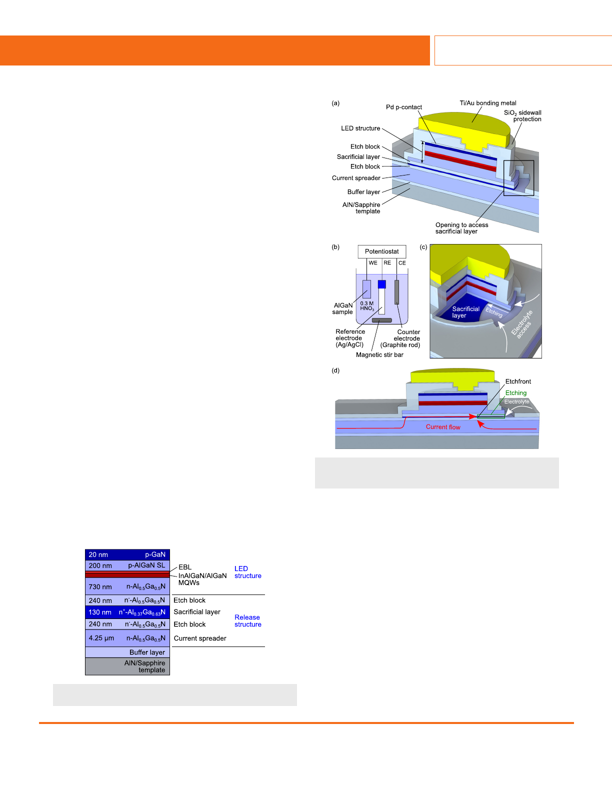
The epitaxial layer structure of the UVB LED including the layers
required for the electrochemical etching is shown in Fig. 1. The structure
was grown in a 3 200 close-coupled showerhead reactor using the
standard precursors trimethylaluminium (TMAl), trimethylgallium
(TMGa), trimethylindium (TMIn), and ammonia (NH
3
)withhydrogen
or nitrogen as the carrier gas. Silane (SiH
4
) was used as a n-dopant
source and cyclopentadienylmagnesium (Cp
2
Mg) as a p-dopant. First,
an AlN/AlGaN-superlattice for strain management was grown on an
AlN/sapphire substrate
13
provided by the Ferdinand-Braun-Institut.
This was followed by a 4 lm thick relaxed silicon doped
Al0:5Ga0:5N-layer with a Si concentration of 2 1018 cm3to complete
the quasi-substrate.
14,26
After that, a 130 nm thick Al0:37Ga0:63N:Si sacri-
ficial layer with a Si-concentration of 2 1019 cm3was sandwiched
between two 240 nm thick Al0:5Ga0:5N:Si etch-stop layers with a
reduced Si-concentration of 0:51018 cm3. On top of that, the
Al0:5Ga0:5N:SicurrentspreadinglayerfortheLEDwasgrown.Thiswas
followed by a threefold InAlGaN MQW active region emitting at
311 nm, an Al0:75Ga0:25N electron blocking layer, and a Mg-doped
AlGaN/AlGaN superlattice with an average Al concentration of 50%
and a Mg concentration of 7 1019 cm3.Finally,thestructurewas
capped by a 20 nm thick GaN:Mg contact layer. The threading disloca-
tion density of the epitaxial layers is around 3 109cm2.
The process flow for the TFFC LEDs is summarized in
Figs. 2(a)–2(d),3(a),and3(b). The fabrication started with the defini-
tion of the LED’s emission area. A circular mesa with a diameter of
80 lm was defined by standard photolithography and chlorine-based
reactive ion etching into the n-doped Al0:5Ga0:5N current spreading
layer of the LED. An additional dry etching step into the bottom n
-
doped Al0:5Ga0:5N-layer, used as the etch stop layer, was performed to
expose the n-doped Al0:37Ga0:63N sacrificial layer. This etch also
definedtheareatobelifted-off.Thecontactpadfortheelectrochemi-
cal etching consisting of Ti/Al/Ti/Au (20/80/40/100 nm) was deposited
on one end of the sample using electron-beam evaporation and
annealed for 1 min at 900 CinaN
2
atmosphere. A 50 nm Pd
p-contact was then evaporated on top of the double mesa and annealed
for 1 min at 550 CintheN
2
atmosphere. To protect the doped epitax-
ial LED layers from parasitic etching during the electrochemical pro-
cess, a SiO
2
layer was deposited on the sample using sputtering. In a
first dry etching step, the SiO
2
layer was etched down beside the mesa
to 300 nm to obtain a thinner tether layer, while its full thickness of
1lm was kept on top of the mesa to create a larger distance between
the mesa top and the sample surface to facilitate bonding. In a second
dry etching step, the SiO
2
layer was opened up at three different loca-
tions: on top of the mesas to access the p-contact layer, at one point at
the mesa edge to expose the sacrificial layer, and on the n-contact pad
used for electrochemical etching. Subsequently, a Ti/Au pad for bond-
ing and contacting was deposited on top of the mesa by tilted e-beam
evaporation. The device structure after the p-side processing is shown
in Fig. 2(a).
FIG. 1. Epitaxial structure of the UVB LED and the layers required for substrate
removal by electrochemical etching.
FIG. 2. (a) Sample structure after the p-side processing, (b) three-electrode setup
for electrochemical etching, (c) sacrificial layer removal, and (d) current flow during
electrochemical etching.
Applied Physics Letters ARTICLE scitation.org/journal/apl
Appl. Phys. Lett. 116, 121101 (2020); doi: 10.1063/1.5143297 116, 121101-2
V
CAuthor(s) 2020
To release the LEDs from the substrate, the sacrificial layer was
laterally removed using electrochemical etching. In this step, the sam-
ple was immersed in 0.3 M nitric acid and electrically connected to a
Biologic potentiostat in a three-electrode setup, see Fig. 2(b). To pre-
vent parasitic etching, the electrical connection to the sample was
protected from the electrolyte. A graphite rod was used as the coun-
ter electrode to drive the required current through the sample in
order to achieve the set potential on the sample relative to the Ag/
AgCl reference electrode. The electrolyte was stirred with a magnetic
stir bar, and etching was conducted at room temperature with no
intentional illumination. An etching voltage of 25 V vs the Ag/AgCl
reference electrode was chosen to achieve complete removal of the
n-doped Al0:37Ga0:63N sacrificial layer, as shown in Ref. 25, and still
to prevent etching of the etch stop and doped device layers. The
lower Al composition and higher doping of the sacrificial layer rela-
tive to the etch block layers on both the sides confine the etching to
only the sacrificial layer. Because the sacrificial layer is only exposed
to the electrolyte at one side of the mesa, the etching proceeds across
the mesa from one direction in one step, see Fig. 2(c). The SiO
2
side-
wall protection further ensures a good current flow throughout the
full electrochemical etch process and constant etching conditions, see
Figs. 2(c) and 2(d). After the etching process, the sample was
immersed in de-ionized water for 1 min to dissolve acid residues and
then immersed in isopropanol to reduce any force on the membrane
when allowed to dry in air. The underetched LEDs were held in place
by the SiO
2
tethers. To flip-chip bond the underetched thin-film
LEDs, thermocompression bonding was used. Prior to the bonding,
the bonding metal surfaces on both the LED devices and the Si car-
rier chip with a Ti/Au (10/300 nm) bonding layer were cleaned by
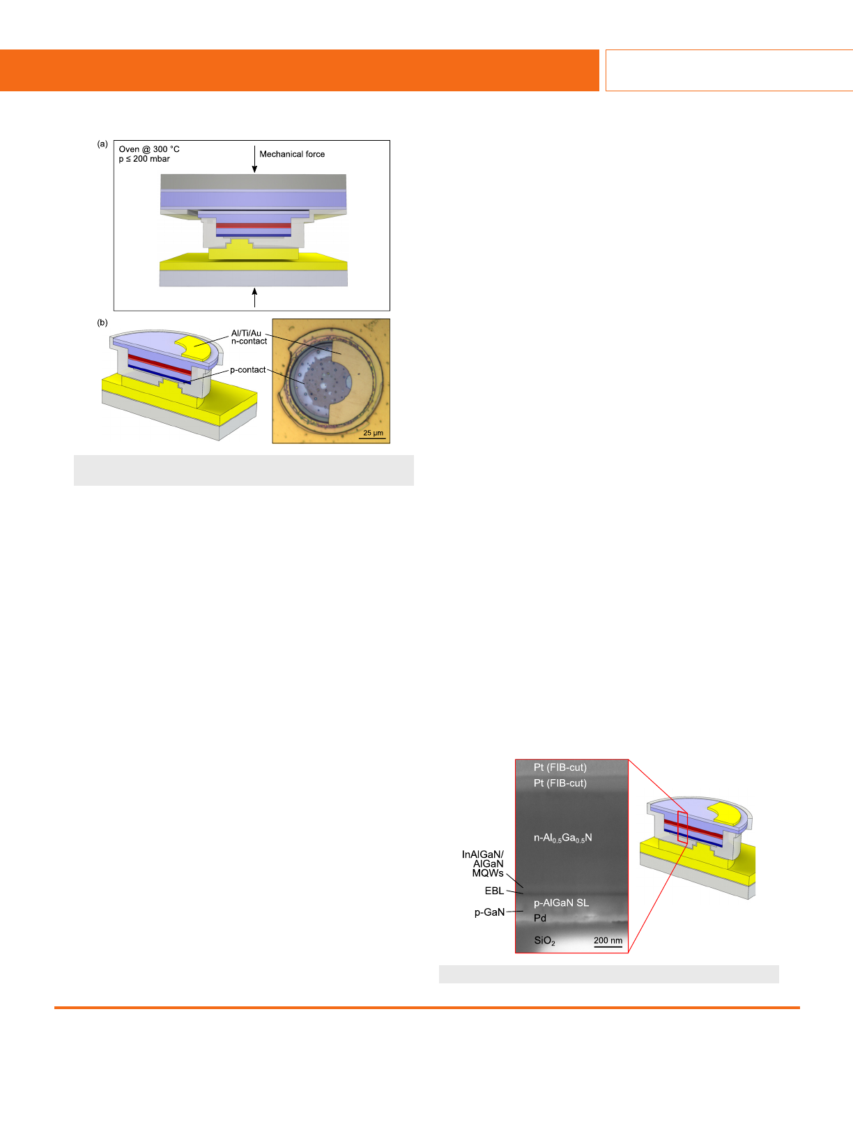
UV-ozone. Subsequently, the chips were pressed together using an
in-house designed stainless-steel compression fixture that was placed
in an oven at 300 C for 2 h, see Fig. 3(a). The bonding pressure on
the bond pad area was set to 50 MPa. To reduce air pockets, the
oven was evacuated to a pressure 200 mbar. During the bonding
process, the SiO
2
tethers break and the thin-film LEDs are trans-
ferred to the Si carrier.
The device process was completed by the formation of an Al/Ti/
Au (100/20/30 nm) n-contact on top of the mesa as shown in the opti-
cal microscope image in Fig. 3(b). An annealing temperature of 550 C
for the n-contact was chosen to minimize the degradation of the
p-contact. The cross-sectional SEM image of the final TFFC LED
achieved by a focused-ion-beam-cut shows well-defined device layers
and indicates a smoothly etched surface as seen in Fig. 4.Moreover,
the device layers show no indication of being porosified by the electro-
chemical etch process. An improper combination of doping levels,
thicknesses, and Al compositions of the LED layers and etch stop layer
in relation to the sacrificial layer and etch voltage would result in
undesired porosification with pore diameters of 50 nm–100 nm,
27
which would clearly be visible in the cross-sectional SEM image. In
addition, time-resolved photoluminescence (PL) measurements
yielded similar PL decay times of 340630 ps at room temperature for
the quantum wells in the as-grown LEDs and in the TFFC LEDs, indi-
cating no degradation of the active region.
25
Figure 5 shows the electroluminescence spectrum at room tem-
perature of the TFFC LED at a current density of 0:8A=cm2with a
single emission peak at 311 nm. This corresponds well to the electrolu-
minescence peak wavelength of 312 nm of the as-grown LED structure
that was contacted using an In-dot, for which the emission was col-
lected through the sapphire substrate. The full width at half maximum
for the TFFC LED is 9 nm and 11 nm for the as-grown LED structure.
Figure 6 shows the voltage and optical output power as a function
of current density for a TFFC LED with a p-contact diameter of
68 lm. The electroluminescence was measured using a broad-area
UV-enhanced Si photodiode S2281 from Hamamatsu. The graph
shows a linear output power vs current density, as expected for an
LED. This proof-of-principle device is not optimized for high light
extraction efficiency, and therefore, the optical output power that is in
the low lW regime is stated in arbitrary units. A homogeneous cur-
rent injection across the p-contact area is assumed when calculating
the current density. However, near-field imaging of the spontaneous
emission at a current of 0:2 mA [see Fig. 7(b)] shows that this is an
underestimation of the current density due to a non-homogeneous
FIG. 3. (a) Flip-chip bonding in the vacuum oven and (b) schematic and optical
microscope image of the thin-flip flip-chip LED before the n-contact annealing.
FIG. 4. Cross-sectional SEM image of the transferred LED structure.
Applied Physics Letters ARTICLE scitation.org/journal/apl
Appl. Phys. Lett. 116, 121101 (2020); doi: 10.1063/1.5143297 116, 121101-3
V
CAuthor(s) 2020
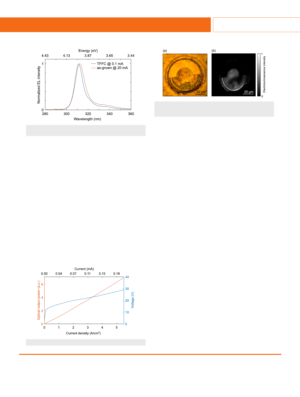
current injection caused by a degraded p-contact. The voltage vs cur-
rent density reveals a high differential resistance of the LED of about
63 kXat 3 A=cm2. This is attributed to a highly resistive n-contact as
the fabrication process was not optimized for the N-polar backside
with low n-type doping, additionally hindered by the limited annealing
temperature to avoid damaging of the LED and possible degradation
of the p-contact. A different process flow, where the n-contact can be
annealed before the p-contact, could solve these issues.
In conclusion, we have demonstrated a thin-film flip-chip UVB
LED where the substrate removal was achieved by lateral electrochemi-
cal etching of an AlGaN sacrificial layer. The LED structure was not
structurally or optically affected by the substrate removal technique,
through a proper design of the sacrificial layer (doping level, thickness,
and Al composition) in relation to the etch stop layer and the device
layers, and choice of the etch voltage. The electroluminescence spec-
trum shows a single peak emission at 311 nm for the thin-film flip-
chip LED, which corresponds to the emission wavelength of the as-
grown LED structure, indicating no significant strain being introduced
or released in the thin-film flip-chip process. The high series resistance
of the LED was attributed to high contact resistance caused by a non-
optimized annealing temperature and n-contacts on low-doped,
N-polar AlGaN. An alternative process flow, where the n-contact is
annealed before the p-contact, should solve this issue. The developed
thin-film process is not limited to UVB LEDs but can also be applied
to deep-UV LEDs and other devices such as UV vertical-cavity sur-
face-emitting lasers that benefit from the integration of high-quality
III-nitride device layers with other structures such as dielectric distrib-
uted Bragg reflectors.
This work was performed in part at Myfab Chalmers. This
project was financially supported by the Swedish Foundation for
Strategic Research, the Swedish Research Council (Project Nos.
2016-04686 and 2018-00295), and the Deutsche
Forschungsgemeinschaft (DFG) within the Collaborative Research
Center “Semiconductor Nanophotonics” (SFB 787).
REFERENCES
1
III-Nitride Ultraviolet Emitters, Springer Series in Materials Science Vol. 227,
edited by M. Kneissl and J. Rass (Springer International Publishing, 2016).
2
M. Kneissl, T.-Y. Seong, J. Han, and H. Amano, “The emergence and prospects
of deep-ultraviolet light-emitting diode technologies,” Nat. Photonics 13,
233–244 (2019).
3
H. Aoshima, K. Takeda, K. Takehara, S. Ito, M. Mori, M. Iwaya, T. Takeuchi,
S. Kamiyama, I. Akasaki, and H. Amano, “Laser lift-off of AlN/sapphire for
UV light-emitting diodes,” Phys. Status Solidi C 9, 753–756 (2012).
4
Y. J. Sung, M.-S. Kim, H. Kim, S. Choi, Y. H. Kim, M.-H. Jung, R.-J. Choi, Y.-
T. Moon, J.-T. Oh, H.-H. Jeong, and G. Y. Yeom, “Light extraction enhance-
ment of AlGaN-based vertical type deep-ultraviolet light-emitting-diodes by
using highly reflective ITO/Al electrode and surface roughening,” Opt. Express
27, 29930–29937 (2019).
5
C. E. Leez, B. S. Cheng, Y. C. Lee, H. C. Kuo, T. C. Lu, and S. C. Wang,
“Output power enhancement of vertical-injection ultraviolet light-emitting
diodes by GaN-free and surface roughness structures,” Electrochem. Solid-
State Lett. 12, H44–H46 (2009).
6
B. K. SaifAddin, A. Almogbel, C. J. Zollner, H. Foronda, A. Alyamani, A.
Albadri, M. Iza, S. Nakamura, S. P. DenBaars, and J. S. Speck, “Fabrication
technology for high light-extraction ultraviolet thin-film flip-chip (UV TFFC)
LEDs grown on SiC,” Semicond. Sci. Technol. 34, 035007 (2019).
7
L. Zhou, J. E. Epler, M. R. Krames, W. Goetz, M. Gherasimova, Z. Ren, J. Han,
M. Kneissl, and N. M. Johnson, “Vertical injection thin-film AlGaN/AlGaN
multiple-quantum-well deep ultraviolet light-emitting diodes,” Appl. Phys.
Lett. 89, 241113 (2006).
8
M. Lachab, F. Asif, B. Zhang, I. Ahmad, A. Heidari, Q. Fareed, V. Adivarahan,
and A. Khan, “Enhancement of light extraction efficiency in sub-300 nm
nitride thin-film flip-chip light-emitting diodes,” Solid-State Electron. 89,
156–160 (2013).
9
M. K. Kelly, O. Ambacher, R. Dimitrov, R. Handschuh, and M. Stutzmann,
“Optical process for liftoff of group III-nitride films,” Phys. Status Solidi A
159, R3–R4 (1997).
FIG. 5. Normalized electroluminescence spectrum of the as-grown epitaxy and the
TFFC LED at room temperature.
FIG. 6. P–I–V characteristics of the TFFC LED.
FIG. 7. (a) Optical microscope image of the TFFC LED and (b) spatially resolved
near-field emission at a current of 0:2 mA. Electroluminescence intensity is on a lin-
ear scale.
Applied Physics Letters ARTICLE scitation.org/journal/apl
Appl. Phys. Lett. 116, 121101 (2020); doi: 10.1063/1.5143297 116, 121101-4
V
CAuthor(s) 2020
Loading more pages...