
Vol.:(0123456789)
https://doi.org/10.1007/s10762-021-00831-5
1 3
Terahertz Multilayer Thickness Measurements: Comparison
ofOptoelectronic Time andFrequency Domain Systems
LarsLiebermeister1 · SimonNellen1 · RobertB.Kohlhaas1 ·
SebastianLauck1· MilanDeumer1 · SteffenBreuer1 · MartinSchell1,2·
BjörnGlobisch1,2
Received: 22 June 2021 / Accepted: 3 November 2021
© The Author(s) 2021
Abstract
We compare a state-of-the-art terahertz (THz) time domain spectroscopy (TDS) sys-
tem and a novel optoelectronic frequency domain spectroscopy (FDS) system with
respect to their performance in layer thickness measurements. We use equal sample
sets, THz optics, and data evaluation methods for both spectrometers. On single-
layer and multi-layer dielectric samples, we found a standard deviation of thickness
measurements below 0.2 µm for TDS and below 0.5µm for FDS. This factor of
approx. two between the accuracy of both systems reproduces well for all samples.
Although the TDS system achieves higher accuracy, FDS systems can be a com-
petitive alternative for two reasons. First, the architecture of an FDS system is essen-
tially simpler, and thus the price can be much lower compared to TDS. Second, an
accuracy below 1µm is sufficient for many real-world applications. Thus, this work
may be a starting point for a comprehensive cross comparison of different terahertz
systems developed for specific industrial applications.
1 Introduction
Terahertz (THz) spectroscopy is an interesting sensing technology for many appli-
cations in material and structural analysis, compound identification, and testing
[1, 2]. The measurement is non-contact and non-destructive, can easily handle air-
material interfaces, and uses non-ionizing radiation. One of the key applications for
THz spectroscopy is the thickness measurements of paint and coating layers. Until
today, time domain spectroscopy (TDS) is almost exclusively used for this kind of
* Lars Liebermeister
[email protected]er.de
1 Fraunhofer Institute forTelecommunications, Heinrich Hertz Institute, Einsteinufer 37,
10587Berlin, Germany
2 Institut Für Festkörperphysik, Technische Universität Berlin, Hardenbergstraße 36, EW 5-1,
10623Berlin, Germany
Journal of Infrared, Millimeter, andTerahertzWaves (2021) 42:1153 1167
–
/Published online: 8 December 2021

1 3
applications, as these systems are mature and commercially available. In addition,
THz TDS offers high acquisition speed and high THz bandwidth. The latter ena-
bles thickness measurements of sub-mm dielectric layers [3–5] and the detection of
defects in polymers, foams, and other non-conductive materials [6].
In contrast, frequency domain spectroscopy (FDS), which is based on the gen-
eration and coherent detection of continuous wave (cw) THz radiation, hitherto is
barely used for non-destructive testing (NDT) [7, 8]. The inherently low measure-
ment rate of most scientific FDS implementations and all commercial FDS prod-
ucts makes NDT with cw THz radiation highly inefficient. However, it was shown
already in 2014 that THz FDS can be used for multilayer thickness measurements
[9]. We have recently demonstrated a THz FDS system that allows acquisition rates
of 200 Hz, which is comparable to the speed of most commercial TDS systems.
With this FDS system, a PET film with a thickness of 23µm could be measured with
an accuracy better than 2%, which corresponds to an uncertainty below 0.5µm. This
demonstrates that FDS can compete with TDS for accurate thickness measurements
on thin dielectric layers [10]. Thereby, the main advantage of FDS compared to TDS
is the simplicity of its system architecture. FDS systems are all-fiber coupled, and
they do not require femtosecond optical pulses, moving optics, or complex phase
locking electronics. This is why many industrial applications may benefit from using
frequency domain spectroscopy instead of TDS. To date, there is no detailed com-
parison between the two methods in terms of measurement accuracy, measurement
time, and reproducibility.
In this paper, we present the first direct comparison of a state-of-the-art TDS and
optoelectronic FDS system for layer thickness measurements in reflection geometry.
Both TDS and FDS measurements were performed on the same samples, namely
PET films with thicknesses between 23 and 350 µm, a Si wafer with a thickness
of 350µm, and a ceramic coated with spray paint on both sides. Based on this, we
compare the ability of the two systems to achieve the same results in consecutive
measurements. Thereby, we analyze the effects of instrument noise, dynamic range,
and bandwidth of the respective system on thickness determination. As the central
figure of merit, we investigated the standard deviation of consecutive measurements
at the same position on the sample. We found that the standard deviation of both
TDS and FDS is always lower than 2%.
This paper is organized as follows: In Section2 we describe in detail the TDS
and FDS system used for the comparison. Section3 explains the experimental setup,
data evaluation, and thickness determination. The measurement results are presented
and discussed in Section4 before we summarize our results in Section5.
2 TDS andFDS System
The TDS measurements in this comparison were done with a commercial state-of-
the-art system, the TeraFlash pro system from TOPTICA Photonics AG [3]. A func-
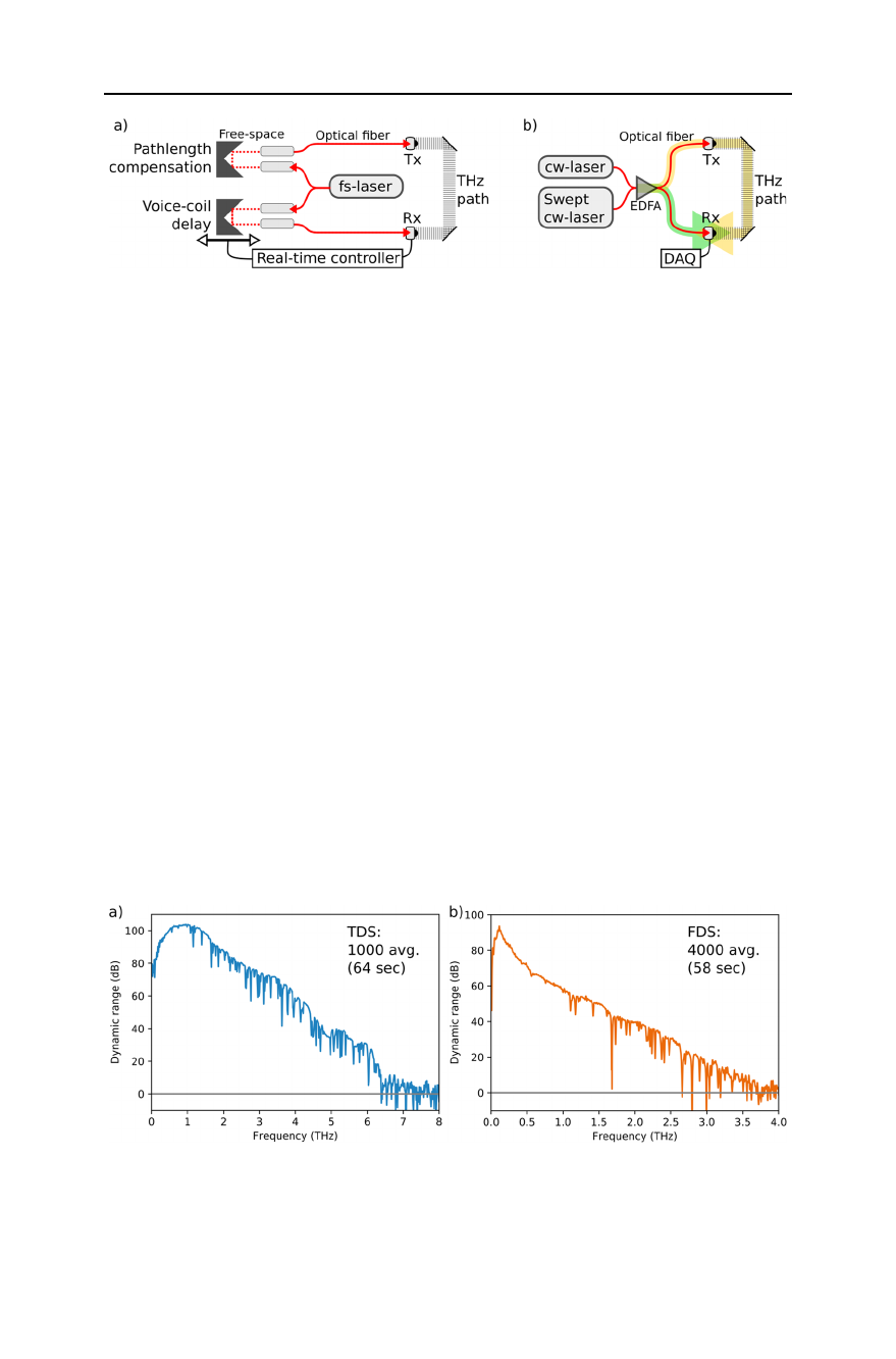
tional diagram of its optical components is shown in Fig.1a. The system uses a fem-
tosecond fiber laser centered at 1560nm, which generates pulses with a duration of
100fs at a repetition rate of 100MHz. A voice-coil driven-optical delay allows for
Journal of Infrared, Millimeter, and Terahertz Waves (2021) 42:1153 1167
–
1154
1 3
time-domain sampling with update rates up to 100Hz. An additional optical delay
line in the receiver arm of the spectrometer allows for compensating a wide range of
THz free space path lengths. Fiber-coupled InGaAs-based photoconductive modules
are used as emitter (Tx) and receiver (Rx), respectively. The photoconductive mate-
rial of the receiver is rhodium-doped InGaAs (InGaAs:Rh) [11, 12]. The Tx uses
iron-doped InGaAs (InGaAs:Fe) [13]. In this configuration, the spectral maximum
of the system is centered at 1THz, and the peak dynamic range reaches 70dB in
single shot (66ms measurement time) and exceeds 95dB for 1000 averages (see
Fig.2a). The total available bandwidth is more than 6THz and the spectral resolu-
tion can be as low as 1GHz. All measurements presented here were acquired with a
scan range of 70ps, corresponding to a spectral resolution of 14GHz.
FDS measurements were performed with a recently published optoelectronic
continuous-wave terahertz spectrometer [10]. The working principle of this sys-
tem is based on frequency-modulated continuous-wave (FMCW), which is an
Fig. 1 Schematics of the two optoelectronic THz spectrometers used in this paper. (a) The TDS system
compromises a pulsed fiber laser (fs-laser), a fast (voice-coil delay) and a slow (path length compensa-
tion) free-space optical delay, photoconductive emitter (Tx) and receiver (Rx), and a real-time control-
ler to drive the voice-coil and acquire the data. All components are fiber-coupled. (b) The FDS system
compromises a fixed-frequency (cw-laser) and a swept laser (Swept cw-laser), an erbium-doped fiber
amplifier (EDFA), a PIN-photodiode emitter (Tx), and a photoconductive receiver (Rx) as well as a
data acquisition unit (DAQ). The Tx- and Rx paths are indicated with yellow- and green-shaded arrows,
respectively. The different path length in the Tx and Rx arm of the spectrometer are a prerequisite for the
optoelectronic FMCW technique [10]
Fig. 2 Comparison of typical spectra recorded with the TDS (a) and FDS (b) systems. The dynamic
range is plotted against frequency. Both records use 1min of averaging. In contrast to the measurements
on the sample, these signals are recorded in a transmission setup consisting of two off-axis parabolic mir-
rors, which is filled with air of ambient humidity
Journal of Infrared, Millimeter, and Terahertz Waves (2021) 42:1153 1167
–
1155

1 3
established technique used in purely electronic THz systems [14]. A schematic dia-
gram of the optoelectronic THz FDS system is shown in Fig. 1b. The spectrom-
eter uses two fiber-coupled, continuous-wave semiconductor lasers emitting in the
c-band (1530–1565nm). The frequency of one of these lasers is swept periodically,
while the emission frequency of the second laser stays fixed. The laser outputs are
spatially overlapped in a 3dB coupler, which generates an optical beat note. This
beat note is amplified by an EDFA before being converted into THz radiation via
photomixing in a waveguide-integrated PIN photodiode [15, 16]. The same beat sig-
nal is also used to drive the coherent detection in the photoconductive Rx [15]. Tx
and Rx are based on commercially available, fiber-coupled modules from TOPTICA
Photonics AG. Further details on the THz FDS system can be found in the litera-
ture [10]. The most significant and fundamental difference of this FDS system com-
pared to common setups with coherent detection of cw THz signals is the method
employed to obtain the phase. When no phase modulation is used, fringe-detection
or Hilbert-transform [17] are common methods to extract the phase information.
Alternatively, active phase modulation by a free-space optical delay line [18], a fiber
stretcher [19], or an optical phase modulator [20, 21] can be employed, which allows
for amplitude and phase determination with a quadrature lock-in detector. The FDS
system used here bases on an optoelectronic adaption of the FMCW technique [10],
which results in passive phase modulation. The tunable cw-laser is frequency swept
with more than 500THz/sec. In combination with a path length imbalance of 20cm
between the emitter and the receiver arm (indicated by shaded arrows), an inter-
mediate frequency of 500kHz is generated in the photomixing receiver, which can
be directly used for coherent detection with a software-based lock-in amplifier. This
quadrature lock-in detection allows to detect amplitude and phase as a function of
frequency. Note that this FDS system neither requires optomechanics nor free space
optics nor electro-optic phase modulation. The THz amplitude spectrum acquired
with the FDS system is depicted in Fig.2b. The spectral maximum is centered at
100GHz with a peak dynamic range exceeding 90dB for 4000averages. In a single
shot measurement, which is acquired in 14ms, the dynamic range measures 60dB
with a 2THz bandwidth. With averaging, the peak dynamic range and bandwidth
can reach 117dB and 4THz, respectively [10]. Figure2 compares the THz spectra
acquired with the TDS and the FDS system for a measurement time around 60s.
3 THz‑Setup andMeasurement Procedure
This section covers the experimental setup, the set of samples, the data preparation,
and the algorithm for thickness determination.
3.1 Experimental Setup
All measurements were carried out in reflection geometry, which is the most
industrially relevant setup. It requires only single-side access to the sample under
test, and reflection measurements can be performed independent of the substrate.
Journal of Infrared, Millimeter, and Terahertz Waves (2021) 42:1153 1167
–
1156
1 3
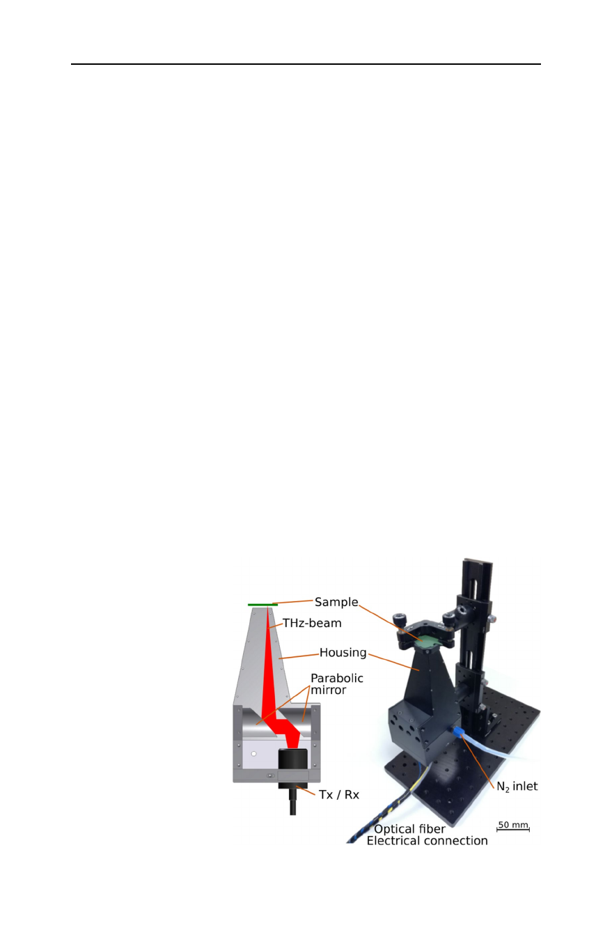
A schematic diagram and photograph of the THz reflection head used for TDS
and FDS measurements are depicted in Fig.3. Since the mechanical dimensions
and beam profile of pulsed and cw emitter and receiver modules are almost identi-
cal, the same THz optical beam path is used for both systems. A 90° off-axis par-
abolic mirror with 2inch focal length collimates the THz beam of the emitter and
another 90°off-axis parabolic mirror with 4inch focal length focuses the beam
on the sample surface under an angle of 8°. The reflected THz beam is collected
and focused on the detector by an equal configuration of mirrors. The diameter
of all parabolic mirrors measures 1inch, which allows for constructing a compa-
rably compact reflection head. The resulting measurement spot is about 1mm in
diameter and the THz-beam is s-polarized with respect to the plane of incidence.
The beam path is oriented upwards (see Fig.3), which allows for placing the sam-
ples reproducibly in the THz focus. In order to suppress THz absorption from
water vapor, the reflection head is encapsulated (housing in Fig.3) and purged
with nitrogen (see photograph in Fig. 3)). Between background, reference, and
sample measurement, the alignment of the reflection head was kept unchanged.
The placement of the sample in the THz-beam path as well as the alignment
is a common cause of variations of the measurement result. This effect can even
dominate the uncertainty of thickness measurements in industrial applications.
However, these variations are mainly related to the geometry of the samples,
the sample holder, the design of the THz optics, and environmental conditions.
Therefore, it is not an effect caused by the THz system used. In our comparison,
we tried to minimize the influence of positioning errors and sample inhomogene-
ity by focusing our analysis on the reproducibility of consecutive measurements
taken on the same position on the sample.
Fig. 3 Schematic and photo-
graph of the reflection head used
for non-contact layer thickness
measurements. The reflection
head was identical for TDS and
FDS measurements. The diam-
eter of the parabolic mirrors
measures 1”. In this view, THz
transmitters and receivers and
their respective beam paths are
arranged one behind the other.
Both beam paths hit the sample
at the same spot and under an
angle of 8°. Tx and Rx have a
distance of 5mm. The housing
is purged with nitrogen to avoid
detrimental effects from water
vapor absorption
Journal of Infrared, Millimeter, and Terahertz Waves (2021) 42:1153 1167
–
1157
Loading more pages...