
Quasi one dimensional transport in individual electrospun composite nanofibers
A. Avnon, B. Wang, S. Zhou, V. Datsyuk, S. Trotsenko, N. Grabbert, and H.-D. Ngo
Citation: AIP Advances 4, 017110 (2014); doi: 10.1063/1.4862168
View online: https://doi.org/10.1063/1.4862168
View Table of Contents: http://aip.scitation.org/toc/adv/4/1
Published by the American Institute of Physics
Articles you may be interested in
Physical origin of nonlinear transport in organic semiconductor at high carrier densities
Journal of Applied Physics 116, 164504 (2014); 10.1063/1.4897916
Nonlinear transport in quasi-one-dimensional Nb2PdS5 nanowires
Applied Physics Letters 105, 172603 (2014); 10.1063/1.4901005

AIP ADVANCES 4, 017110 (2014)
Quasi one dimensional transport in individual electrospun
composite nanofibers
A. Avnon,1,aB. Wang,2S. Zhou,2V. Datsyuk,1S. Trotsenko,1N. Grabbert,3
and H.-D. Ngo3
1Institut f¨
ur Experimentalphysik, Freie Universit¨
at Berlin, Arnimallee 14, 14195 Berlin,
Germany
2Research Center of Microperipheric Technologies, Technische Universit¨
at Berlin, TiB4/2-1,
Gustav-Meyer-Allee 25, 13355 Berlin, Germany
3Microsystem Engineering (FB I), University of Applied Sciences, Wilhelminenhofstr.
74 (C 525), 12459 Berlin, Germany
(Received 17 November 2013; accepted 30 December 2013; published online 9 January 2014)
We present results of transport measurements of individual suspended electrospun
nanofibers Poly(methyl methacrylate)-multiwalled carbon nanotubes. The nanofiber
is comprised of highly aligned consecutive multiwalled carbon nanotubes. We
have confirmed that at the range temperature from room temperature down to
∼60 K, the conductance behaves as power-law of temperature with an exponent of
α∼2.9−10.2. The current also behaves as power law of voltage with an exponent
of β∼2.3−8.6. The power-law behavior is a footprint for one dimensional trans-
port. The possible models of this confined system are discussed. Using the model
of Luttinger liquid states in series, we calculated the exponent for tunneling into
the bulk of a single multiwalled carbon nanotube αbulk ∼0.06 which agrees with
theoretical predictions. C
2014 Author(s). All article content, except where other-
wise noted, is licensed under a Creative Commons Attribution 3.0 Unported License.
[http://dx.doi.org/10.1063/1.4862168]
As nanosized devices are becoming more and more significant, electron-electron interactions
due to the size confinement, become more important for transport and worthy of consideration and
discussion. Electron-electron interactions are a main player in one dimensional transport bringing
about behavior different from the classic Fermi liquid. Different kinds of behaviors are associ-
ated with electron-electron interactions: Luttinger liquid behavior resulting from repulsive short
range electron-electron interactions,1–5Wigner crystal behavior resulting from long range Coulomb
interaction6or environmental Coulomb blockade.7The characteristic fingerprint for quasi- one di-
mensional behavior is a power-law dependence of the conductance with temperature and of the
current with applied potential. The power-law was observed in various systems ranging from carbon
nanotubes,1–3,6–8conducting conjugated polymer nanowires,5,9–11 semiconductors nanowires4,12,13
and fractional quantum Hall edge states.14
One way of obtaining continuous nanofibers is by electrospinning.15,16 During the process, the
nanofibers can be filled with nanosized fillers, resulting in highly aligned one dimensional nanofibers.
In that respect, it is a unique system which creates a long nanochain of confined conduction. Doping
insulating polymers such as Poly(methyl methacrylate) (PMMA) with multiwalled carbon nanotubes
(MWCNTs) creates a confined one dimensional system. This system can present either short range
or long range electron-electron interactions depending on the temperature and morphology which
can further elucidate the nature of one dimensional behavior.
In this paper, we report our transport studies of individual suspended electrospun MWCNT-
PMMA nanofiber. We perform analysis of early experimental data for a MWCNT-PMMA nanofiber
aCorresponding author; electronic address: [email protected]
2158-3226/2014/4(1)/017110/6 C
Author(s) 20144, 017110-1
017110-2 Avnon
et al.
AIP Advances 4, 017110 (2014)
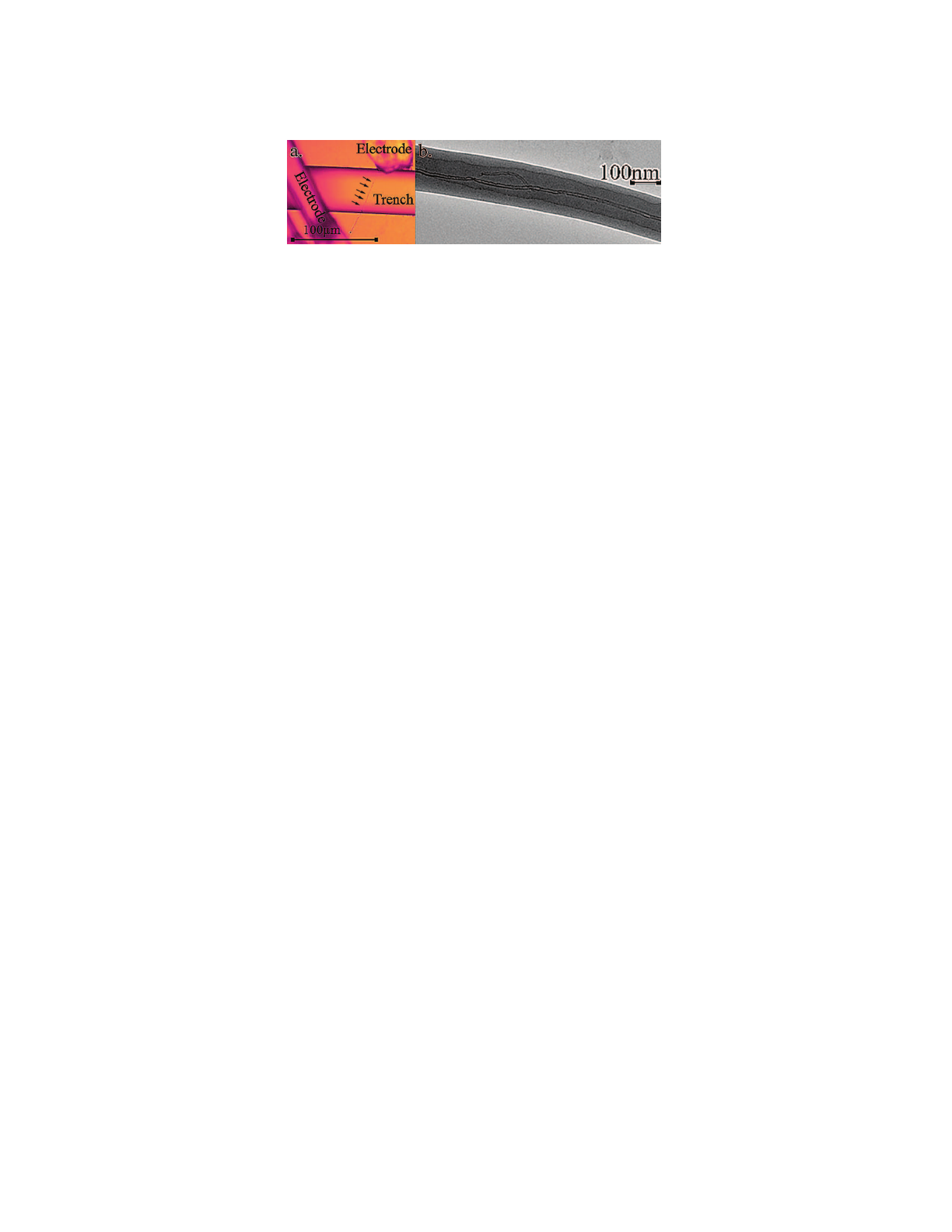
FIG. 1. (a). Optical image of a representing individual MWCNT-PMMA nanofiber. The nanofiber is visible as a faint black
line over the trench and is connected by direct bonds. To assist the eye, the image was sharpened and arrows are pointing at
the nanofiber. It can be seen that only a single nanofiber is nested across the trench. The trench width is 50 μm. The total
length of the nanofiber between the bonds is ∼100 μm. (b). A transmission electron microscopy image of the nanofiber. The
MWCNTs align inside the nanofiber in series and create a nanochain of conduction with minimal separation.
aiming to determine the adaptation of different models for one dimensional conductors and in
particular the model for Luttinger liquid states in series.
We fabricated three samples. Two samples with 20 wt% of MWCNTs and one sample with
25 wt% of MWCNTs. For the first two samples, we dispersed 0.6g of MWCNTs purchased from
Bayer Material Science -Baytubes C15015,17 in 60g of dimethyl acetamide (Carl Roth, GMbH)
with 1g of hydroxypropyl cellulose (from Aldrich Mw 100.000) by ultrasonification for 30 minutes.
3g of PMMA (from Aldrich Mw 996.000) were dissolved in 30g of acetone. Dimethyl acetamide
and acetone were used without any additional purification. For dispersion tip sonicator Sonopuls
HD3100, Bandelin GmbH, equipped with a cup horn operating at 10 kHz and 100 W output power
was used.16 Components were mixed together and were dispersed by ultrasonification for additional
30 minutes. Nanofibers were electrospun using Yflow R
2.2.D-300 lab -scale electrospinning unit
with single-nozzle electrospinning (Yflow Sistemas y Desarrollos S.L) with an injector-collector
distance of 15 cm, an applied voltage of +9.5/−8.0 kV, and a flow rate of 2 ml/h. For the third
sample we used 25 wt% of MWCNTs with flow rate of 1 ml/h, applied voltage of +8/−12 kV and
injector-collector distance of 12 cm.
For electrical conductivity study, nanofibers were spun directly onto a highly doped Si/SiOx sub-
strate with 600nm oxide with prefabricated trenches. For the fabrication of the trenches, 100mm100
wafers with one polished side were used. A cleaning process was performed using H2SO4+H2O2.
After this, a photolithography process was performed. The resist thickness was 1.5 μm. Trenches
in width of 50 μm were etched using deep silicon etching followed by resist stripping and another
cycle of H2SO4+H2O2cleaning. For the insulation of the substrate, a 600 nm thick SiO2layer was
deposited on the wafer using wet oxidation at 1000oC. Candidate nanofibers were located using
an optical microscope and afterward were connected through direct aluminum bonding onto the
nanofibers. Atomic force microscopy imaging was performed with Park XE-150 in tapping mode
to determine the diameter of the nanofibers. The electrical measurements were performed with a
Keithley 4200-SCS and an Oxford closed cycle cryostat with 2-probe in Helium ambiance.
Fig. 1(a) presents an image of our device taken with an optical microscope. The nanofibers
can be seen as faint black lines running between the electrodes. The total length of each nanofiber
as estimated from the optical microscope are ∼100 μm in average. From atomic force microscopy
images we estimated the diameter of a single nanofiber as ∼120 nm. The average length of MWCNT
is ∼1.5 μm. Fig. 1(b) shows a transmission electron microscopy image of the nanofiber. It can be
seen that the MWCNTs align inside the nanofiber in series and create a nanochain of conduction
with minimal separation. We have three working devices in total. Two working devices out of 25
devices from one sample that were fabricated with 20 wt% MWCNTs and one working device out of
51 devices from two samples that were fabricated with with 25 wt% MWCNTs. The results for the
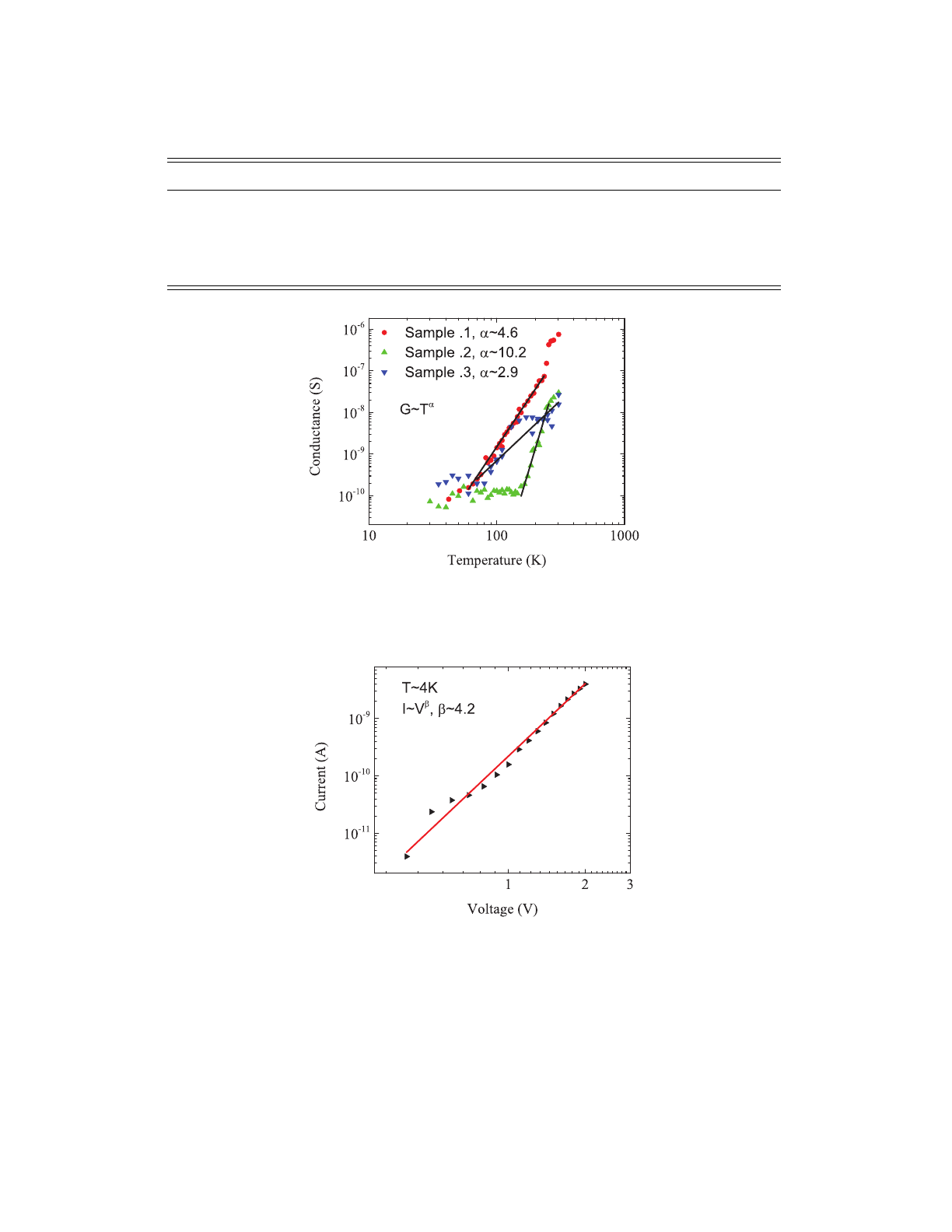
devices discussed, are presented in Fig. 2and summarized in Table I.Fig.2shows the conductance
as a function of temperature. As can be seen, the conductance follows a power-law behavior G(T)
∝Tαover a large temperature range as long as the condition eV kBTis satisfied. For highly
resistive devices such as device 2. the drop of the conductance is fast and already in relatively high
temperatures the current can no longer be detected. Repeated measurements reveal a Kondo-like
behavior in low temperatures and is described elsewhere.25 This may indicate a highly resistive joint
017110-3 Avnon
et al.
AIP Advances 4, 017110 (2014)
TABLE I. Values for nanofibers used in transport experiments.
Device 1. Device 2. Device 3.
MWCNT % in nanofibers 20 20 25
α4.6 10.2 2.9
βat min T 4.2 8.6 2.3
G305K (S) 7.5 ·10−73·10−82.67 ·10−8
Diameter (nm) 120 120 120
FIG. 2. Conductance vs. temperature for the working devices. The black lines are a fit over the results at high temperatures
as expected from the condition eV kBT. All devices obey power-law behavior where in highly resistive devices25 such
as in device .2 the conductance drops quickly below the threshold sensitivity of the system. Table Ipresents the values
corresponding to the samples.
FIG. 3. I-V characteristics at 4K. As can been seen, the power-law behavior of the current under large potential eV kBT
is retained. The red line is a fit of the data with voltages above 0.4 V.
creating a small detachment in the nanochain of conduction. However, device 2. in high temperatures
still obeys power-law behavior.
Fig. 3shows that also the I-V characteristics retain power-law behavior I(V)∝Vβat low
temperature where eV kBTis satisfied. Similar behavior exists in polymer fibers,9–11 carbon
nanotubes,1–3,8quantum Hall edge states,14 and other inorganic one dimensional nanowires.4,12,13
In carbon nanotube/polymer composite nanofibers beyond a concentration percolation
threshold,18 the electrical conductivity rises sharply to saturation. The dependence between
the electrical conductivity to nanotube alignment also obeys similar rules. Beyond the critical

017110-4 Avnon
et al.
AIP Advances 4, 017110 (2014)
alignment threshold18 the electrical conductivity shows a sharp rise with respect to the degree of
carbon nanotube alignment. For highly aligned carbon nanotubes in composite nanofibers, the onset
of percolation pathway begins from loading above 3 wt%.18 As our loading is 20–25 wt%, we stand
well above this threshold. Therefore, the electrospinning process created a nanochain of MWCNTs
separated by minimal tunneling barriers (Fig. 1). Hence, we can expect a quasi-one dimensional
behavior. However, the length and the morphology of each nanofiber in consideration does not
necessarily mean that it would behave similarly to MWCNTs or that the power-law fashion would
mean a long nanochain of Luttinger liquid states in series (Fig. 1).
For the confined system we have, there are a few models to consider. The first option is one
dimensional variable range hopping19,20 and fluctuation induced tunneling.21 They predict ln G
∼−1/Tp, which contradict the temperature dependence observed experimentally. The discrepancy
between our results to the fluctuation induced tunneling21,22 model exemplifies the fact that the
separation between the consecutive MWCNTs is minimal (Fig. 1). For three-dimensional disordered
system23 in the critical regime of the metal-insulator transition, the temperature dependence of the
resistivity follows a universal power-law σ(T)∼Tγwith 0.33 <γ <1. In our case all power-law
exponents exceed unity (Table I) and therefore this model is invalid. We also rule out space-charge
limited current24 where I∼Vβwith β∼2. According to our fits β2 (Table Iand Fig. 3), which
is in contradiction to this explanation.
Turning to the model of Wigner crystal- it is caused by long range Coulomb interaction and
occurs in solids with a dilute system of electrons such as carbon nanotubes6where the Coulomb
energy ECis bigger than the kinetic energy of the electrons EF. As our structure is comprised of
consecutive MWCNTs divided by tunneling barriers and impurities (Fig. 1) -this morphology can
easily create potential wells where electrons get trapped and create Wigner crystal. Every Wigner
crystal state would be pinned down by the tunneling insulating barriers, impurities and kinks.
However, since each potential well is essentially a MWCNT with small energy gap (<100 meV),
it would be difficult to observe any Wigner crystal state. At this time, we cannot fully explore
this behavior at low temperature. A classical Wigner crystal, on the other hand, would require an
exponential relation for the conductance with temperature19 in low temperatures and one dimensional
variable range hopping behavior. This is not recorded in our system.
To be consistent with Luttinger liquid behavior the system must follow a few requirements:
power-law of the current under large potential eV kBTand of the conductance at small potential
eV kBT. The number of the channels in the nanofiber decide on the power-law parameters of β
and α. More generally, the Luttinger liquid model states the current depends1–3,6,8on voltage and
temperature as
I=I0Tα+1sinh(eV/kBT)|(1 +β/2+ieV/πkBT)|2,(1)
where is the Gamma function, I0is a constant, and αand βare the power-law parameters
introduced above. Fig. 4shows how at low temperatures the current follows a universal curve. This
agrees with the Luttinger liquid model described by Eq. (1). The Luttinger liquid model characterizes
a system by its interaction parameter gderived from the tunneling density of states.1,3For strong
repulsive electron-electron interactions, g1 while for non interacting electrons, g=1. According
to Luttinger liquid theory predictions for a system where impurity and kink barriers are dominant α
follows:
α∼(g−1−1)/4.(2)
We estimate g1∼0.04, g2∼0.02, g3∼0.08 respectively for the devices under consideration
(A similar value can be reached also for intertube tunneling). This indicates a strong repulsive
electron-electron interactions regime in the nanofibers.
For a single conduction channel, e.g. at low temperatures where only few channels survive and
are active, the correlation between the power-law exponents is
β=1+α. (3)
In our measurements βis always lower than α+1 as already observed in inorganic nanowires
and polymer nanowires.9,12 The absolute values of αand βdetermined by us are also higher
Loading more pages...