
Assembly of carbon nanotubes and alkylated fullerenes: nanocarbon hybrid
towards photovoltaic applications†
Yanfei Shen,*
a
Juan Sebasti
an Reparaz,
b
Markus Raphael Wagner,
b
Axel Hoffmann,
b
Christian Thomsen,
b
Jeong-O Lee,
c
Sebastian Heeg,
d
Benjamin Hatting,
d
Stephanie Reich,
d
Akinori Saeki,
e
Shu Seki,
e
Kaname Yoshida,
f
Sukumaran Santhosh Babu,
a
Helmuth M€
ohwald
g
and Takashi Nakanishi*
a
Received 13th June 2011, Accepted 28th July 2011
DOI: 10.1039/c1sc00360g
Taking advantage of the non-covalent interaction between alkyl chains and the sidewalls of a single-
walled carbon nanotube (SWCNT), a nanocarbon hybrid of SWCNT and a fullerene (C
60
) derivative
with long alkyl chains was constructed as a donor–acceptor pair for photovoltaics and nanodevice
investigations. It was found that SWCNT could be mostly unbundled by the alkylated C
60
(1) and was
well-dispersed in organic solvents. As a photoactive material, the resultant nanocarbon hybrid, 1-
SWCNT, performed well in light-energy harvesting applications in photoelectrochemical cells and
nanoscale field-effect transistors (FET). Moreover, the 1-SWCNT assembly exhibited
superhydrophobicity, providing an interesting opportunity to fabricate nanocarbon-based waterproof
optoelectronic devices. In order to understand the photoexcitation process, the 1-SWCNT assembly
was electrochemically and spectroscopically characterized. The electrochemical results showed that the
SWCNT facilitated electronic communication between 1and the electrode. The steady-state and time-
resolved fluorescence and the photoluminescence excitation studies suggested efficient quenching of the
singlet excited state of C
60
. Nanosecond transient absorption data revealed the one-electron reduction
of fullerene, C
60
_
, thereby demonstrating the photoinduced electron transfer from SWCNT to the C
60
unit in the 1-SWCNT assembly.
1. Introduction
Since the discovery of carbon nanoclusters, such as single-walled
carbon nanotubes (SWCNT) and fullerenes (e.g. C
60
), the use of
nanocarbon science, including in organic synthesis,
1–3
supra-
molecular material chemistry,
4–10
surface nanotechnology
11
and
nanoelectronics,
12,13
has rapidly developed. SWCNTs have
emerged as attractive candidates for the development of light-
energy harvesting and photovoltaic materials because of their
unique structure and the presence of extended p-delocalization.
14
Of these, SWCNT-based nanohybrids formed by electron
donor–acceptor systems have been the focus of attention.
15,16
The
association with electron donors or acceptors can modulate the
electronic properties of SWCNTs and results in new potential
materials.
On the other hand, fullerene (C
60
) has a highly delocalized 3D p-
system and its properties have been intensively investigated in
recent years. Among its most spectacular physical and chemical
properties, C
60
was found to be able to reversibly accept up to six
electrons, behave as a strong electron acceptor and show excep-
tional electronic absorption bands expanding throughout the entire
UV-vis wavelength range.
17
The extraordinary electron acceptor
properties have resulted in noteworthy advances in the research
areas of light-induced electron transfer and solar energy conver-
sion.
18–21
Therefore, the hybridization of C
60
with SWCNTs
5,7,22–27
would couple the optical and electronic properties of SWCNTs
together with the electron-acceptor feature of C
60
.
Covalent modification is one of the strategies for the attach-
ment of C
60
onto sidewall of SWCNT.
28,29
However, this partly
disrupts their electronic structure and carrier transport proper-
ties. As an alternative, non-covalent functionalization has been
developed. The ability to fabricate nanocarbon assemblies, which
are potentially exploitable for the bottom-up construction of
nanodevices, demands the development of general and reliable
approaches to control the self-assembly processes. To this end,
a
National Institute for Materials Science (NIMS), 1-2-1 Sengen, Tsukuba,
nims.go.jp; Tel: +81-(0)29-860-4740
b
Technische Universit€
at Berlin, 10623 Berlin, Germany
c
Korea Research Institute of Chemical Technology, Daejeon, 305-343,
Korea
d
Freie Universit€
at Berlin, 14195 Berlin, Germany
e
Graduate School of Engineering, Osaka University, Osaka, Japan
f
Institute for Chemical Science, Kyoto University, Japan
g
Max Planck Institute of Colloids and Interfaces, 14424 Potsdam,
Germany
† Electronic supplementary information (ESI) available: HR-TEM,
Raman, DSC, AFM, SEM, solution photographs, IPCE, steady-state
and time-resolved fluorescence spectra. See DOI: 10.1039/c1sc00360g
This journal is ªThe Royal Society of Chemistry 2011 Chem. Sci., 2011, 2, 2243–2250 | 2243
Dynamic Article LinksC
<
Chemical Science
Cite this: Chem. Sci., 2011, 2, 2243
www.rsc.org/chemicalscience EDGE ARTICLE
Published on 25 August 2011. Downloaded on 01/04/2016 07:27:25.
View Article Online
/ Journal Homepage
/ Table of Contents for this issue

applying p–pstacking interactions with C
60
or polyaromatic
substituents on C
60
towards the periphery of SWCNTs has been
well-established.
5,7,30
Here, we report a facile, versatile and non-destructive way to
construct nanocarbon hybrids by alkyl chain-assisted assembly
between an alkylated C
60
derivative 1
31,32
and SWCNTs (Scheme
1). The appropriate affinity of long aliphatic chains of 1towards
a SWCNT surface allows the solubilization of SWCNTs in
organic solvents without disturbing their intrinsic electronic
structures.
33
The solubility of SWCNTs with the assistance of 1,
maintaining electronic communication between them, makes it
suitable for photovoltaic studies and field-effect transistor (FET)
fabrication via wet processes. To grasp a deeper understanding of
the photoenergy conversion process, we also performed
a detailed spectroscopic study of the photoinduced electron
transfer between the two components. In addition, the obtained
nanocarbon assembly exhibits water repellency at its surface,
which provides an extra benefit for the photovoltaic application,
i.e., for the fabrication of waterproof devices.
2. Experimental
2.1 Materials
C
60
derivatives 1–5 and 3,4,5-eicosyloxy benzaldehyde 6were
synthesized by following our previous synthetic procedure.
34
Briefly, C
60
derivatives were prepared by refluxing the corre-
sponding benzaldehyde with N-methylglycine and C
60
in dry
monochlorobenzene. SWCNT (Super Purified grade, Unidym)
produced by high-pressure decomposition of carbon monoxide
(HiPco process) were used as received.
2.2 Preparation of 1-SWCNT composite solution
The mixture of 1(3.5 mg) and SWCNT (1 mg) was firstly grinded
in a mortar, and then transferred to THF (8 mL) in a vial and
followed by ultrasonication for about 6 h using the Branson 5510
ultrasonic equipment (40 kHz). The solution was subsequently
centrifuged (Force Micro 1618) at 10000 rpm for 40 min, and
two-thirds of the resultant supernatant liquid was decanted
carefully from the settled solid. To get the ratio of SWCNT in the
nanohybrids, 1was firstly washed out from the 1-SWCNT
nanohybrids through PTFE filter paper (Whatman, pore size
0.45 mm) with THF. The resulting SWCNT on filter paper was
dried at 80 C in a vacuum and weighed on an ultra-fine balance.
The weight ratio of SWCNTS to 1-SWCNT nanohybrids was
calculated to be about 18% from the obtained SWCNT weight
and the amount of 1added for preparing the nanohybrids. After
evaporating the solvent from the as-obtained supernatant liquid,
the solid 1-SWCNT was used for HR-TEM analysis. The
supernatant liquid was used directly for spectroscopy charac-
terizations, i.e., UV-vis–NIR, steady-state fluorescence, time-
resolved fluorescence, photoluminenscence, transient absorption
studies and photoelectrochemical measurements. UV-vis–NIR
spectra were recorded with a Jasco V570 spectrophotometer.
2.3 Electrochemical and photoelectrochemical measurements
Electrochemical experiments were conducted in a classic three-
electrode system using a Garmy Reference 600 Potentiostat/
Galvanostat/ZRA Instrument. The working electrode was
a glassy carbon electrode, auxiliary and reference electrodes were
a Pt ring and Ag/AgCl (saturated KCl), respectively. A thin film
of 1-SWCNT on a glassy carbon electrode was prepared by
depositing the 1-SWCNT supernatant liquid (10 mL) followed by
drying in air for 24 h. Differential pulse (pulse amplitude 25 mV)
voltammograms (DPV) of the cast film of 1-SWCNT were
performed in 0.1 M aqueous n-Bu
4
NCl solution at 70 C. Pho-
toelectrochemical measurements were carried out in a two-elec-
trode system with 1-SWCNT/FTO, 1/FTO or SWCNT/FTO as
the working electrode and a Pt wire as the counter electrode. The
aggregation of 1-SWCNT and 1for photoelectrochemical
measurements was obtained by rapid injection of an equivalent
volume of methanol to a THF solution of 1-SWCNT and 1(the
concentration of 1was 0.2 mM). The electrodes were prepared by
casting methods. The short-circuit current was measured by
immersing the working electrode and counter electrode into the
electrolyte solution containing LiI (0.5 M) and I
2
(0.01 M) in
acetonitrile. A 150 W Xe lamp (Asahi Spectra, USA) equipped
with a LAX-Cute Airmass 1.5 G filter was used as the light
source. The incident light intensity was focused and calibrated to
1 Sun (1000 W m
2
) by a 1 sun checker. The modified area of the
working electrode (0.2 cm
2
) was illuminated from the back.
2.4 FET device fabrication and measurements
SWCNTs were grown on Si wafers with 500 nm-thick SiO
2
. The
liquid catalyst, consisting of Fe(NO
3
)
2
$9H
2
O, alumina nano-
powder and Mo(acac)
2
in methanol, was dispersed onto the
substrates with patterned poly(methyl metacrylate). After lifting
this off, the SWCNT was grown by heating to 900 C in a furnace
with CH
4
as the carbon feedstock. Patterns for electrical leads
were made with photolithography and the thermal evaporation
of Ti and Au. The channel length between the source and drain
electrodes was 5 or 7 mm. Electrical transport measurements were
done in a custom-built probe station with Lab View-controlled
electronics. Photoexcitation experiments were performed using
an Osram halogen lamp (12 V, 100 W) equipped with a micro-
scope in the probe station.
2.5 Characterization
High-resolution transmission electron microscopy (HR-TEM)
images were obtained by a JEOL transmission electron micro-
scope, model JEM2200FS. Solid 1-SWCNT assemblies were
dispersed in chloroform with ultrasonication. One drop of the
solution was deposited on an electron microscopy microgrid and
the sample was carefully rinsed with THF to show the clear visual
state of the assembly, especially the debundled SWCNTs, before
Scheme 1 The molecular structures of 1–6 and SWCNT.
2244 | Chem. Sci., 2011, 2, 2243–2250 This journal is ªThe Royal Society of Chemistry 2011
Published on 25 August 2011. Downloaded on 01/04/2016 07:27:25.
View Article Online
TEM measurements were carried out. All of the TEM images
were recorded by a CCD camera with an accelerating voltage of
200 kV. Scanning electron microscopy (SEM) images were
recorded by means of a Philips XL30 electron microscope at an
accelerating voltage of 3 kV.
Flash-photolysis time-resolved microwave conductivity
(TRMC) measurements of 1-SWCNT and 1were carried out
using an X-band (9 GHz) microwave circuit at low power
(approximately 3 mW) and a nanosecond laser irradiation at
355 nm with a photon density of 9.1 10
15
cm
2
.
35
Samples for
TRMC measurements were prepared by evaporating the THF
solution of 1-SWCNT and 1followed by drying the solid samples
at 70 C in a vacuum for about 5 h. The solid samples were pasted
on a quartz plate with double-sided sticky tape (the tape does not
disturb any TRMC signal). The smooth film was formed by
physical smoothing with a spatula and used for TRMC
measurements.
Photoluminescence excitation (PLE) data was acquired using
a HORIBA Jobin Yvon Fluorolog-3 spectrofluorometer. A
HeXe broadband lamp served as the excitation source. The PLE
map was recorded in steps of 5 nm in excitation with an acqui-
sition time of 20 s. The luminescence data was normalized with
respect to the light source using a Si diode as the reference. The
spectrometer response was taken into account by comparison
with a known reference source. Photoluminescence (PL) spectra
were collected using a HORIBA Jobin Yvon Fluorolog spec-
trometer equipped with 450 W of a Xenon arc lamp and 350 mm
of focal point distance for the excitation monochromator. Slits
for the excitation and emission monochromaters were fixed at
4 nm for the excitation and 4 nm for the emission mono-
chromator and the integration time was 0.5 s. For the time-
resolved PL measurements, the samples were excited using the
second harmonic of a Ti sapphire laser with a pulse length of
2 ps. The excitation wavelength was tuned to 400 nm (3.1 eV).
Transients were recorded by single photon counting using
a Hamamatsu R3809U-52 microchannel plate (MCP). The
emitted light was dispersed by a subtractive double mono-
chromator with a spectral resolution of 0.1 nm. The instrumental
time resolution was limited by the time walk of the MCP of about
30 ps, which allows the determination of lifetimes down to 10 ps
using deconvolution techniques.
The nanosecond transient absorption measurement in the
range 530–900 nm were performed by a monochromator,
a streak camera and a continuous Xe lamp, while the one for
900–1600 nm was done by a monochromator, an InGaAs pin
photodetector and a Xe flash lamp. The third harmonic gener-
ation (355 nm) of a nanosecond Nd : YAG laser was used as an
irradiation laser. The THF solutions were saturated with N
2
before measurements were carried out.
3. Results and discussion
3.1 Assembly of SWCNT with 1
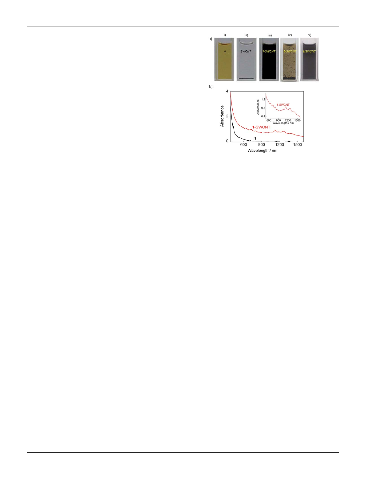
The interaction between 1and SWCNTs allows the unbundling
and dispersion of SWCNTs in organic solvents, such as tetra-
hydrofuran (THF) (Fig. 1a) and chloroform (CHCl
3
) (Fig. S1†).
As revealed in Fig. 1b, the well-resolved absorption peaks in the
UV-vis–NIR spectrum of 1-SWCNT in THF suggest the
presence of SWCNTs with small bundles
8,9
and the preservation
of the intrinsic electronic structure of the SWCNTs after the
assembly with 1. The unbundling of SWCNTs was also sup-
ported by the high-resolution transmission electron microscopy
(HR-TEM) analysis (Fig. S2†). In addition, as indicated by the
arrows in the TEM image, several spherical objects with
a diameter of approximately 1 nm close to the sidewall of the
nanotubes are observed, which are likely to be C
60
derivatives
attached onto thin bundles of SWCNTs.
It is interesting to know which moiety (C
60
or aliphatic chains)
of 1has the stronger affinity with the SWCNT sidewalls. To
investigate this point, control experiments (Fig. 1a) were per-
formed with 5and 6(Scheme 1), which are molecules containing
the C
60
unit and alkyl substituent moiety of 1, respectively. It was
found that 6has better performance than 5in dispersing pristine
SWCNTs, suggesting a more favorable affinity of long alkyl
chains towards the sidewalls of SWCNTs in organic solvents.
Apart from this control experiment, other C
60
derivatives with
a shorter alkyl chain length (2) or a lower number of alkyl chains
(3,4) can also disperse SWCNTs well (Fig. S3†), showing the
capability of other various task-specific molecules to manipulate
assemblies. This result is consistent with our previous report that
alkylated C
60
can align on the surface of graphite forming
perfectly straight C
60
nanowires,
36,37
due to good lattice matching
between the graphite and the all-trans conformation of the oligo-
methylene units.
38
Therefore, driven by the interaction between
the long alkyl chains of C
60
derivatives and SWCNTs, the
nanocarbon assemblies of alkylated C
60
-SWCNT were success-
fully prepared. Alkylated C
60
-SWCNT assemblies are therefore
expected to be a potential candidate for the wet-process fabri-
cation of nanocarbon-based optoelectronic devices. While this
non-covalent functionalization can more effectively preserve the
intrinsic electronic features of SWCNT compared to covalent
methodology, sonication during the sample preparation may
Fig. 1 a) Photographs of 1(i), SWCNT in the absence (ii) and presence
(iii) of 1and in the presence of 5(iv) and 6(v) in THF; b) UV-vis–NIR
absorption spectra of 1and 1-SWCNT in THF; the inset shows an
enlarged area between 570–1500 nm showing the van Hove singularities.
The concentration of 1and SWCNTs are 0.25 mM and 0.125 mg ml
1
,
respectively.
This journal is ªThe Royal Society of Chemistry 2011 Chem. Sci., 2011, 2, 2243–2250 | 2245
Published on 25 August 2011. Downloaded on 01/04/2016 07:27:25.
View Article Online
cause shortened carbon nanotubes or defects along the sidewall
(see the Raman spectra in Fig. S4†).
3.2 Electrochemical properties of 1-SWCNT assembly
It is known that SWCNTs have been widely utilized as a con-
ducting channel to build a number of nanoscale electronic
devices by chemical modification with various inorganic
12
and
organic
39
semiconductors due to the unique electronic properties.
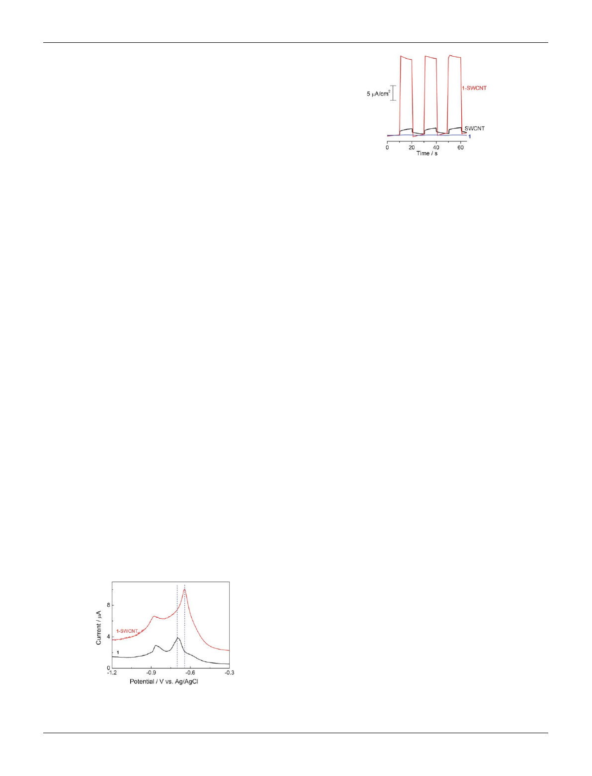
As shown in Fig. 2, the cast film of 1on a glassy carbon electrode
in 0.1 M aqueous n-Bu
4
NCl solution at 70 C exhibits two redox
waves corresponding to the generation of C
60
mono- and di-
anions at potentials of E
red
,
1
697 mV and E
red
,
2
865 mV vs.
Ag/AgCl, respectively.
40
1is in a fluid-mesophase at 70 C, which
facilitates the diffusion of molecules (e.g. the supporting elec-
trolyte, solvent and C
60
molecules) throughout the system. In
comparison, in the nanocarbon hybrid film of 1-SWCNT under
the same conditions (see the differential scanning calorimetry
(DSC) result in Fig. S5†), the first reductive peak positively shifts
by approximately 50 mV and the peak intensity increases by
a factor of 2. This result suggests that SWCNTs facilitate the
electronic communication between 1and the electrode surface.
The enhanced electrochemical activity is attributed to the unique
electronic properties of SWCNTs, which offers a better electron
transfer pathway. This electrochemical result also provides
additional positive evidence for the assembly of 1and SWCNTs.
In addition, the interaction between 1and SWCNTs was also
supported by the DSC result (See Fig. S5†).
3.3 Photoelectric conversion of 1-SWCNT assembly
Using the standard photoelectrochemical (PEC) cell configura-
tion is a fundamental and facile method to evaluate the photo-
energy conversion of semiconducting materials.
41
Accordingly,
photocurrent measurements were performed in a PEC cell
(Fig. S6†) in acetonitrile containing LiI (0.5 M) and I
2
(0.01 M),
employing 1-SWCNT-coated FTO (1-SWCNT/FTO) as
a working electrode and a Pt wire as a counter electrode. Fig. 3
shows the short-circuit photocurrent generation of 1-SWCNT/
FTO upon excitation with white light. The anodic photocurrent
response is prompt, steady and reproducible. Moreover, the
photocurrent of 1-SWCNT/FTO is much larger than that of
either 1/FTO (>160 fold) or SWCNT/FTO (>18 fold). The
incident photon-to-electron conversion efficiency (IPCE) is
calculated to be about 5% at 405 nm (see more discussion in Figs
S7 and S8†). The direct interaction between 1and the SWCNT
could be a factor for driving away the charge carriers to the
collecting surface, where the one-dimensional architecture of
SWCNTs facilitates charge transport and charge collection.
16
A
particular advantage of our nanocarbon hybrid is the ease of
nanodevice fabrication by simply cast/spin-coating from a vola-
tile solution containing 1-SWCNT, which is desirable for
industrial applications. Further improvements in the efficiency
can be expected by varying the ratio of C
60
derivative/SWCNT in
the hybrids,
16
increasing the C
60
content in the derivative by
reducing the aliphatic chain volume, photoelectrochemical cell
optimization and/or the addition of a third component, such as
an appropriate electron donor.
42
For instance, the IPCE value
was enhanced from 3% to 5% upon optimising the SWCNT
content in the hybrid from 10 wt% to 18 wt%.
Single-SWCNT devices show excellent electronic properties,
such as photoconductivity, and therefore have recently received
much attention.
43,44
Here, the photoinduced electron transport
properties of the 1-SWCNT assembly were investigated by using
a single-SWCNT-FET device (Fig. 4a). SWCNT-FETs were
fabricated using patterned chemical vapour deposition (CVD)
and photolithography (see details in the Experimental section).
The decoration was performed by immersing SWCNT-FETs in
a THF solution of 1(1 mM) for about 1 s and rinsing with fresh
THF, forming 40–120 nm-sized clusters of 1along SWCNT
surfaces (Fig. S9†). Fig. 4b shows the evolution of gate transfer
characteristics upon decoration with 1, followed by photo-
excitation. Without the decoration of 1, the SWCNT-FET (black
squares) shows ambipolar characteristics (finite n-channel
conductance). However, after assembly treatment with 1, the 1-
decorated SWCNT-FET (red circles) shows unipolar p-type
transport, with the gate threshold voltage positively shifting by
5 V. This p-type characteristic is attributed to the charge
transfer between 1and local parts of the SWCNTs, suggesting
that 1exerts a strong electron acceptor effect on the SWCNTs.
The p-channel current decreases upon decoration of 1, which is
probably due to the enhanced scattering. Moreover, upon illu-
mination with light (11.3 mW), a further hole doping effect is
observed and the device does not show complete depletion of
conductance (empty red circles). In contrast, the bare SWCNT-
FET (control experiment) shows almost no difference in the
photoresponse (empty black squares). Fig. 4c shows the I–V
characteristics of the device upon illumination. A gate voltage of
2 V was applied to the device to intentionally turn it off. In the
Fig. 2 Differential pulse voltammograms (pulse amplitude 25 mV) of
a cast film of 1-SWCNT and 1on a glassy carbon electrode (0.1 M
aqueous n-Bu
4
NCl solution, at 70 C).
Fig. 3 The short-circuit photocurrent response of 1/FTO, SWCNT/
FTO and 1-SWCNT/FTO under white light (150 W Xe lamp). The
electrolyte was 0.5 M LiI and 0.01 M I
2
in acetonitrile and the counter
electrode is a platinum wire.
2246 | Chem. Sci., 2011, 2, 2243–2250 This journal is ªThe Royal Society of Chemistry 2011
Published on 25 August 2011. Downloaded on 01/04/2016 07:27:25.
View Article Online
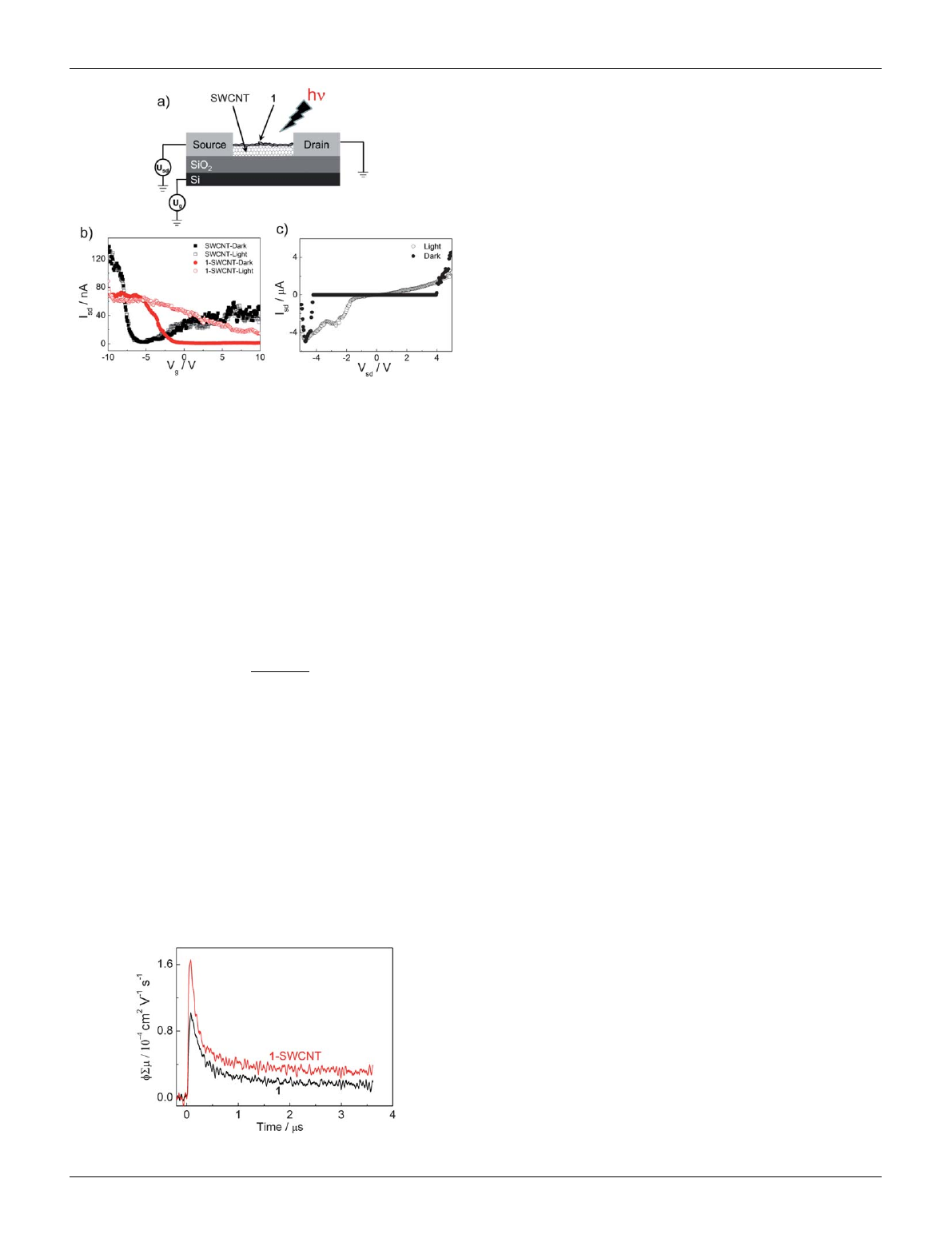
dark state, the device was turned off and electronic conduction
occurred only at high bias (>4 V) voltages (black circles). In
contrast, upon illumination with light, a quasi-linear transport
characteristic appears (open circles in Fig. 4c). The optical
responsivity (R) of the device was estimated to be about 7 10
4
at 3 V bias according to the following formula:
45
R¼Ilight=IDark
Powerlamp
(1)
where I
light
and I
dark
are 2.99 10
6
and 3.79 10
9
A,
respectively. Furthermore, the device shows a reproducible
photoresponse (Fig. S10†). Therefore, the current result shows
that the 1-decorated SWCNT-FET can be used as excellent
photosensing and solar energy converting nanodevices.
The photoelectric conversion performance of 1-SWCNT is
supported by the photoconductivity evaluation via a flash-
photolysis time-resolved microwave conductivity (TRMC)
technique.
35
Fig. 5 shows the transient photoconductivity (fPm,
where frepresents the quantum efficiency of the charge carrier
generation and Pmrepresents the sum of the nanometre-scale
charge carrier mobilities) of 1-SWCNT and 1upon 355 nm laser-
pulse irradiation. In the presence of SWCNTs, the fPmvalue
increased by about 60% (1.6 10
4
cm
2
V
1
s
1
) compared to
that of 1. Therefore, the increased photoconductivity supports
the electron communication in the 1-SWCNT assembly, which is
consistent with the FET result.
Additionally, the 1-SWCNT assembly provides an anti-
wetting surface, which is highly desirable for practical applica-
tions. The scanning electron microscopy (SEM) image
(Fig. S11†) shows that the surface of the SWCNT is fully coated
with the assembled 1and exhibits a different thickness and
roughness at both the nano- and micrometre scales. The
hydrophobicity of 1, combined with the surface roughness of
SWCNT, renders the 1-SWCNT assembly superhydrophobic,
with a static water contact angle (CA) of 154(Fig. S11a†). In
contrast, the surface of the SWCNT film without 1has a CA of
only 104(Fig. S11b†). The superhydrophobic films of 1-
SWCNT possess high durability under a variety of environ-
mental conditions, such as in various acidities, basicities, ionic
strengths and polar solvents (Fig. S12†). Superhydrophobicity of
nanocarbon materials
8
would be beneficial for any applications
in optoelectronic devices, by reducing the influence of water on
their performance.
3.4 Steady-state fluorescence and photoluminescence
excitation studies
Since the photoexcitation process of 1-SWCNT is crucial in the
photovoltaic system, steady-state fluorescence experiments were
performed. Fig. 6a shows the steady-state fluorescence of 1in the
absence (curve i) and presence (curve ii) of the SWCNTs in
CHCl
3
. In both cases, 1exhibits a single transition at 712 nm.
The fluorescence intensity of 1-SWCNT relative to that of 1is
reduced by 55%. Similar results were obtained in THF solution
(Fig. S13a†), suggesting the occurrence of an interaction between
the excited state of 1and the SWCNTs.
To obtain more information on the interaction between 1and
SWCNT in the excited state, photoluminescence excitation
(PLE) mapping studies of SWCNTs in the near infrared (NIR)
region were performed for the 1-SWCNT assembly in THF
(Fig. 6b). For comparison, we also measured the PLE spectrum
of the SWCNTs in SDS aqueous solution (Fig. 6c), where chiral
indices of (9,4), (7,6), (8,4), (10,2), (7,5), (8,3), (9,2), (6,5) and
(10,3) were observed.
46
The emission from 1-SWCNT solution is
relatively weaker than that of SWCNT-SDS. Since the PL
intensity of the SWCNTs decreases with the externally applied
potential,
47
the weaker emission could be additional evidence for
excited-stated events between 1and SWCNTs. In addition, the
absorption of 1in the visible region and the small bundles of
SWCNTs in solution might also weaken the emission of
SWCNTs.
3.5 Time-resolved fluorescence and nanosecond transient
absorption studies
The excited state dynamics of 1-SWCNT was further investi-
gated by using picosecond time-resolved spectroscopy. As shown
in Fig. 7a, the fluorescence decay of 1in CHCl
3
(red) can be
represented by a single-exponential function with a lifetime of
Fig. 4 a) A schematic illustration of the photoconductivity experiment
using a FET equipped with a single SWCNT with the decoration of 1;b)
the evolution of the gate transfer (I
sd
-V
g
) characteristics of 1-decorated
SWCNT-FET with and without light illumination and those of the
SWCNT-FET with and without light illumination, bias voltages V
sd
¼
100 mV; c) the I
sd
-V
sd
characteristics of the 1-decorated SWCNT-FET
device with and without light illumination (at V
g
¼2 V).
Fig. 5 The TRMC kinetics of 1and 1-SWCNT.
This journal is ªThe Royal Society of Chemistry 2011 Chem. Sci., 2011, 2, 2243–2250 | 2247
Published on 25 August 2011. Downloaded on 01/04/2016 07:27:25.
View Article Online
Loading more pages...