Semiconductor Science and Technology
Semicond. Sci. Technol. 37 (2022) 105016 (8pp) https://doi.org/10.1088/1361-6641/ac8e8f
Electrical properties and microstructure
of V/Al/Ni/Au contacts on
n-Al0.65Ga0.35N:Si with different Au
thicknesses and annealing temperatures
H K Cho1,∗, A Mogilatenko1, N Susilo2, I Ostermay1, S Seifert1, T Wernicke2,
M Kneissl1,2and S Einfeldt1
1Ferdinand-Braun-Institut, Gustav-Kirchhoff-Str. 4, 12489 Berlin, Germany
2Technische Universität Berlin, Institute of Solid State Physics, Hardenberg-Str. 36, 10623 Berlin,
Germany
E-mail: hyunk[email protected]
Received 12 May 2022, revised 8 August 2022
Accepted for publication 1 September 2022
Published 9 September 2022
Abstract
We investigated the formation of ohmic contacts as a result of intermetallic phase formation
between V, Al, Ni, and Au in V/Al/Ni/Au metal stacks on n-Al0.65Ga0.35N:Si. In particular, the
influence of Au metal thickness and annealing temperature was analysed. The lowest annealing
temperature of 750 ◦C for an ohmic contact with a smooth surface and a contact resistivity of
about 2.4 ×10⁻⁵Ωcm2was achieved for V(15 nm)/Al(120 nm)/Ni(20 nm)/Au(40 nm). The
lowest contact resistivity is accompanied by formation of two thin interfacial regions consisting
of AlN and an Au-rich phase. We suggest that not only the formation of thin interfacial AlN
layer is important for a low contact resistance, but also the formation of the Au-rich interface
can have a favourable effect on the contact properties.
Keywords: ohmic contact, n-AlGaN, high Al mole fraction, UV LED, Au rich phase, AlN
(Some figures may appear in colour only in the online journal)
1. Introduction
Al-rich n-type AlGaN has been attracting significant atten-
tion because it is needed for ultraviolet light emitting diodes
(UV LEDs) used for sterilization, water purification, and med-
ical diagnostics [1,2]. Hence, several efforts have been made
to understand the contact formation mechanisms to Al-rich
n-AlGaN in order to achieve low resistance contacts [3–10].
Concepts for ohmic contacts developed for n-GaN also work
∗Author to whom any correspondence should be addressed.
Original content from this work may be used under the terms
of the Creative Commons Attribution 4.0 licence. Any fur-
ther distribution of this work must maintain attribution to the author(s) and the
title of the work, journal citation and DOI.
for Ga-rich n-AlGaN [11–13]. Here, Ti/Al-based metal stacks
are typically used [14]. However, for Al-rich n-AlGaN, this
type of contact is associated with a high potential barrier at
the metal–AlGaN interface [15,16] resulting in a significant
nonlinearity of the current–voltage characteristics. As the Al
mole fraction in n-AlGaN is increased, these contacts become
more and more resistive and rectifying.
V/Al-based contacts were proposed for Al-rich AlGaN [4].
These contacts can be processed at a lower temperature and
provide a lower contact resistance than Ti/Al-based contacts
[8]. A thin nitride layer (typically VN or AlN) has been found
to form at the corresponding metal–AlGaN interface [4,8,10].
Although not yet proven, it is nevertheless assumed that nitro-
gen atoms from AlGaN participate in the formation of this thin
nitride layer, and that nitrogen vacancies created in AlGaN
near the metal interface during this reaction act as donors. As
1361-6641/22/105016+8$33.00 Printed in the UK 1 © 2022 The Author(s). Published by IOP Publishing Ltd
Semicond. Sci. Technol. 37 (2022) 105016 H K Cho et al
a result, the increased donor concentration near the interface
would reduce the width of the Schottky barrier and promote the
tunneling of electrons. Up to now, V/Al-based metallizations
with a Ni, Pd, Pt, or Mo diffusion barrier on top have been
reported [4,6]. A final Au cap layer is beneficial to reduce
the sheet resistance of the contact and to limit oxidation [4,
8]. Besides that, it was found that the optimum V/Al thick-
ness ratio is likely to be affected by the other elements (Ni
or Au) present in the metal stack [8]. In addition, an increas-
ing Al mole fraction in the AlGaN requires an increasing
annealing temperature to achieve the lowest possible contact
resistivity [9,10].
While a number of chemical phases are known to form at
the interface (VN, AlN, AlOx, and Au) [8,10], the reason
for the ohmic behavior of a contact with an optimum V/Al
thickness ratio, an optimum Au cap layer thickness, and an
optimum annealing process is still unclear. Therefore, a more
comprehensive analysis is required. Here, we present a study
on the electrical and microstructural properties of V/Al/Ni/Au
contacts with varying thickness of the Au cap layer annealed
under different conditions.
2. Experimental
AlGaN heterostructures were grown by metal–organic
vapour phase epitaxy (MOVPE) on c-plane sapphire
substrates. First, a 500 nm thick AlN layer on sap-
phire was patterned into stripes by photolithography and
dry etching and then epitaxially laterally overgrown by
AlN to a total thickness of 6 µm [17]. Subsequently, a
900 nm thick Al0.76Ga0.24N:Si current spreading layer,
a 100 nm Al0.76Ga0.24N:Si →Al0.65Ga0.35N:Si transition
layer with gradually changing composition and a 500 nm
Al0.65Ga0.35N:Si (∼5×1018 cm−3) contact layer were grown
[18]. The concentration of Si dopants in AlGaN was evaluated
by secondary-ion mass spectrometry.
Test structures for determination of the specific contact res-
istance by the linear transmission line method (TLM) were
fabricated by a lift-off process. First, 200 nm of the surface
were etched using a mixture of BCl3and Cl2at a pressure
of 1 Pa in an inductively coupled plasma-reactive ion etch-
ing system. An oxygen plasma was used to remove possible
residues after photoresist development. Prior to the depos-
ition of the n-contact metal stack, the plasma-etched surfaces
were treated in HCl/H2O (1:1) at room temperature for 30 s,
rinsed in de-ionized water for 1 min and spin-dryed under
nitrogen. Thereafter, two metal layer stacks with different Au
thickness, i.e. V(15 nm)/Al(120 nm)/Ni(20 nm)/Au(20 nm)
and V(15 nm)/Al(120 nm)/Ni(20 nm)/Au(40 nm), were depos-
ited by electron-beam evaporation and structured by a lift-off
process. The contacts were annealed at a maximum anneal-
ing temperature ranging from 700 ◦C to 850 ◦C in nitrogen
ambient for 30 s using a rapid thermal annealing (RTA) fur-
nace. Different annealing temperatures were tested on separ-
ate samples. Only the annealing at 850 ◦C was carried out after
previous annealing at 800 ◦C. In addition, the heating speed
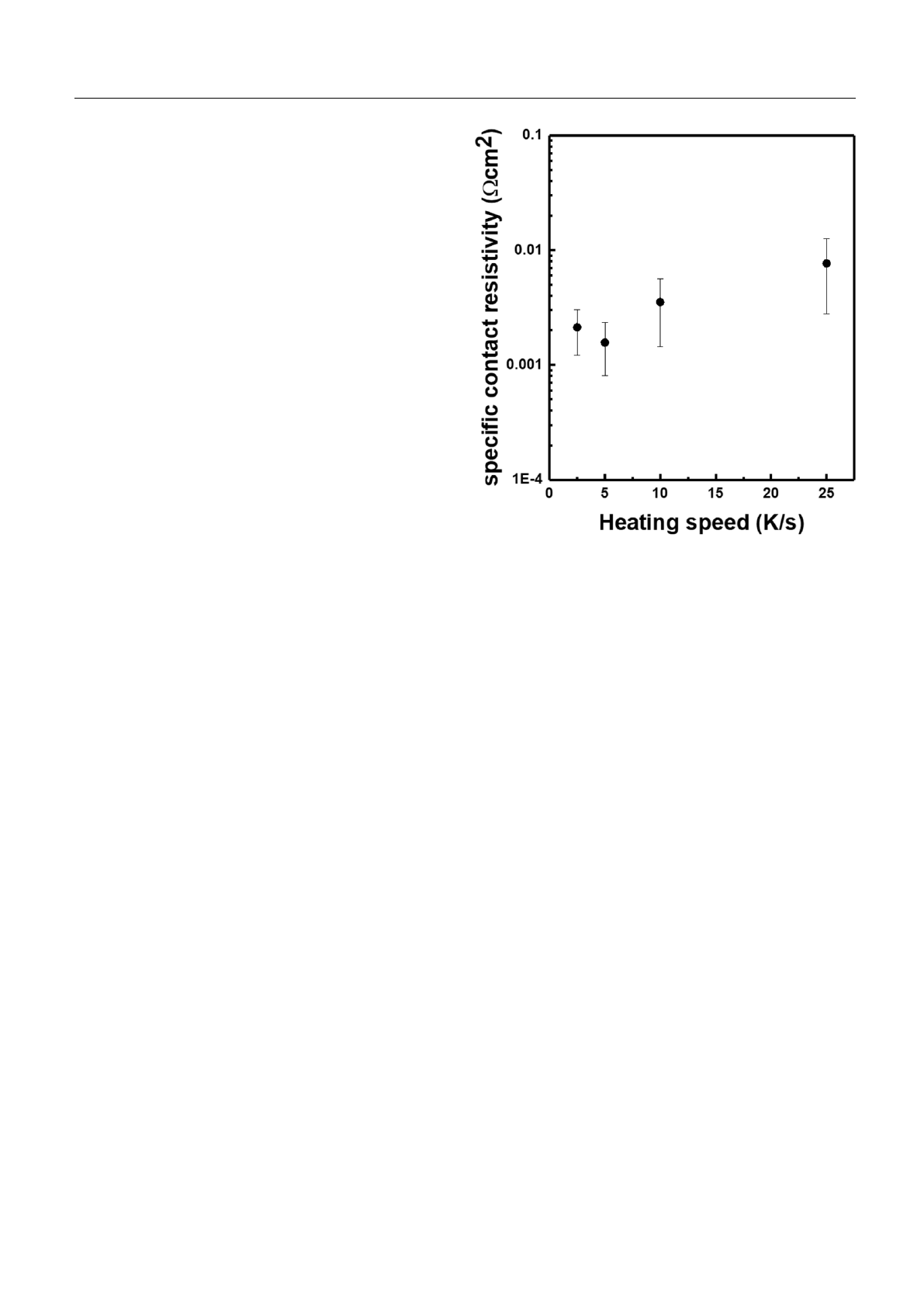
Figure 1. Specific contact resistivity of V(15 nm)/Al(120 nm)/
Ni(20 nm)/Au(20 nm) contacts on n-Al0.65Ga0.35N:Si formed after
annealing at 750 ◦C for 30 s using different heating speeds. Specific
contact resistivities derived from TLM measurements at a current of
1 mA for the two metal systems.
was varied between 2.5 K s−1and 25 K s−1. The contacts had
a size of 460 µm×100 µm and spacings of 10 µm, 15 µm,
20 µm, 25 µm, and 30 µm, respectively. Current–voltage
(I–V) measurements were performed at room temperature.
The surface morphology of the metal contacts was
examined by scanning electron microscopy (SEM). Cross-
section transmission electron microscopy (TEM) samples
were prepared to examine the phase formation in the metal
layer stack after annealing. High resolution TEM (HRTEM)
using broad parallel beam illumination and high angle annu-
lar dark-field scanning TEM (HAADF STEM) in combination
with energy dispersive x-ray (EDX) spectroscopy and electron
energy loss spectroscopy (EELS) were performed to reveal
the structure and the compositional uniformity of the metal–
semiconductor interface.
3. Results and discussion
Figure 1shows the specific contact resistivity of
V(15 nm)/Al(120 nm)/Ni(20 nm)/Au(20 nm) contacts
obtained for different temperature ramp rates from room tem-
perature to the maximum temperature of 750 ◦C. The lowest
contact resistivities are obtained for the slowest temperature
ramp rates of 2.5 K s−1and 5 K s−1. This indicates that for a
low contact resistivity, diffusion processes (presumably of the
contact metals) must take place to a sufficient extent. This is
only given if the time available for diffusion is long enough,
2
Semicond. Sci. Technol. 37 (2022) 105016 H K Cho et al
Figure 2. I–Vcurves from two-point measurements between contacts of 20 µm distance on n-Al0.65Ga0.35N:Si obtained after annealing at
different temperatures (a) V(15 nm)/Al(120 nm)/Ni(20 nm)/Au(20 nm), and (b) V(15 nm)/Al(120 nm)/Ni(20 nm)/Au(40 nm). (c) Specific
contact resistivities derived from TLM measurements at a current of 1 mA for the two metal systems.
Figure 3. Top-view SEM images of metal contacts on Al0.65Ga0.35N:Si annealed at different temperatures: (a)–(c) V(15 nm)/Al(120 nm)/
Ni(20 nm)/Au(20 nm), and (d)–(f) V(15 nm)/Al(120 nm)/Ni(20 nm)/Au(40 nm).
i.e. here if the ramp rate is small enough. Therefore, all fol-
lowing annealing experiments have been performed with a
heating speed of 5 K s−1.
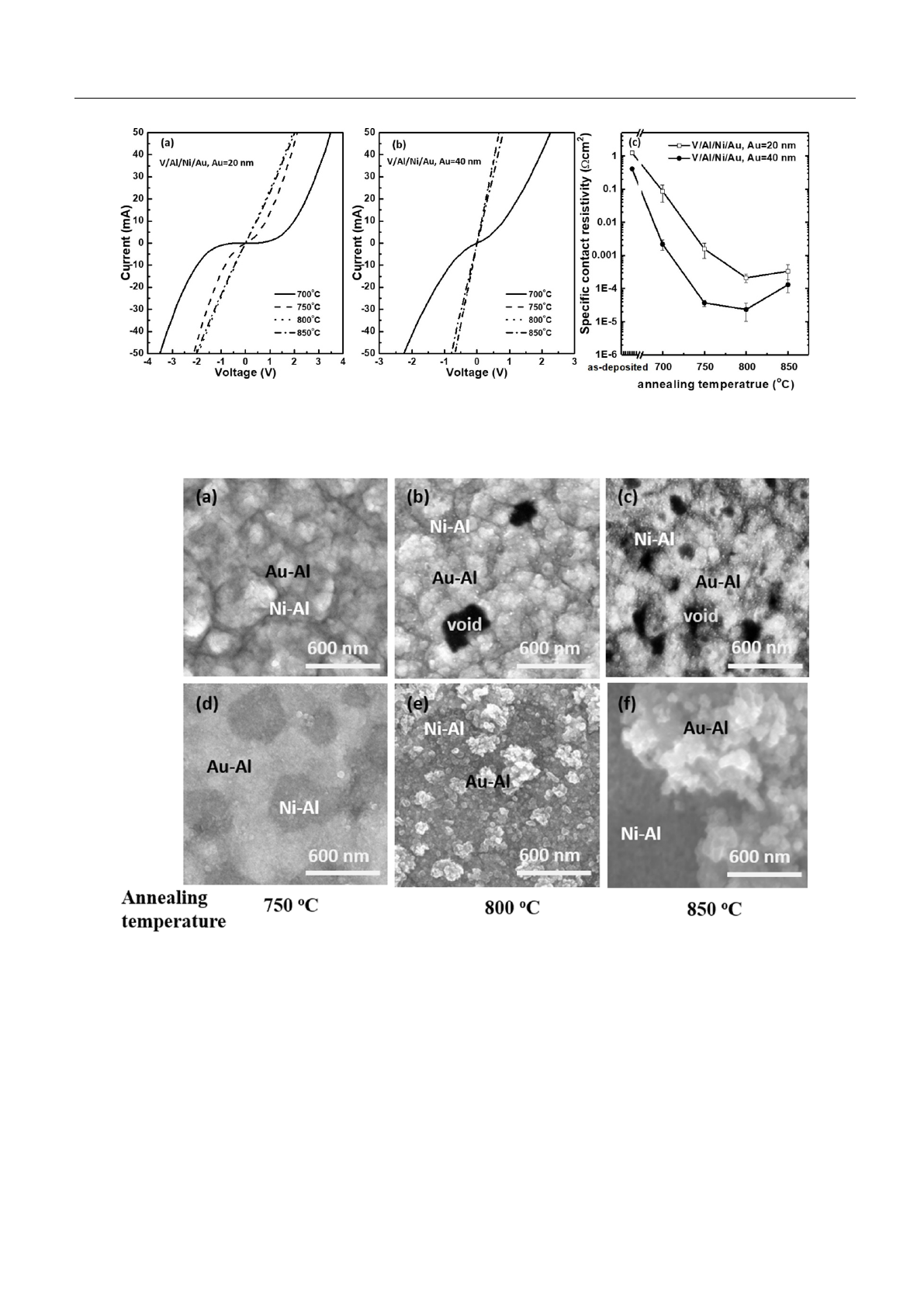
Figures 2(a) and (b) show the I–Vcurves of the two types
of contacts for different maximum annealing temperatures.
Also, the corresponding specific contact resistivities derived
from TLM measurements are shown in figure 2(c). The as-
deposited contacts (not shown here) are rectifying. By increas-
ing the annealing temperature, the I–Vcharacteristics become
linear after annealing beyond 800 ◦C (figure 2(a)) and 750 ◦C
(figure 2(b)), respectively. A minimum specific contact res-
istivity is reached around 800 ◦C for both Au thicknesses, i.e.
2.1 ×10⁻⁴Ωcm2and 2.4 ×10⁻⁵Ωcm2, for a Au thickness
of 20 nm and 40 nm, respectively.
The morphology and composition of the contact surfaces
was studied by SEM (figure 3) and EDX (figures 4and 5).
Figure 3shows the comparison of the surface morphology of
the two sets of samples (with 20 nm and 40 nm Au cap layer)
3
Semicond. Sci. Technol. 37 (2022) 105016 H K Cho et al
Figure 4. (a) SEM bird’s eye view of a FIB cut in a V(15 nm)/Al(120 nm)/Ni(20 nm)/Au(20 nm) contact after annealing at 850 ◦C (inset in
the lower corner shows a magnified image of a void in the layer); (b) top-view SEM image (b) and corresponding EDX map (c) showing the
distribution of Au-M and Ni-L peak intensities (V-K and Al-K maps showed a uniform intensity distribution and thus are not shown here).
Figure 5. Top-view SEM images (a), (d) and EDX maps (b), (c), (e), (f) acquired at V(15 nm)/Al(120 nm)/Ni(20 nm)/Au(40 nm) contacts
after annealing at 750 ◦C (a)–(c) and 850 ◦C (d)–(f), respectively.
4

Semicond. Sci. Technol. 37 (2022) 105016 H K Cho et al
after annealing at different temperatures. Up to an anneal-
ing temperature of 750 ◦C, the surface of both metallization
stacks remains relatively smooth (figures 3(a) and (d)). How-
ever, when further increasing the annealing temperature up
to 850 ◦C, the surface morphology changes. For the 20 nm
thick Au cap layer voids are formed at 800 ◦C. Their number
increases with increasing annealing temperature, as shown in
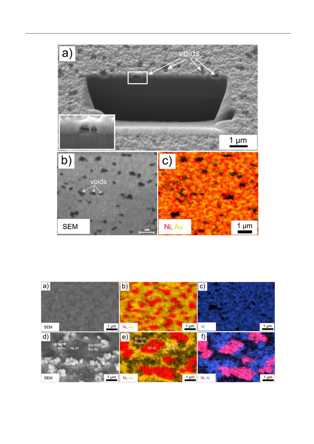
figures 3(b) and (c). In particular, focused ion beam (FIB) was
used to prove the formation of voids in the contact layers after
annealing at 850 ◦C (figure 4(a)). EDX maps show a uniform
distribution of small grains in this sample which correspond
to two phases: Ni–Al and Au–Al (for Au and Ni signal see
figure 4(c), the Al and V signals were uniformly distributed
and thus are not shown here). Obviously, for a Au cap layer
thickness of 20 nm elevated annealing temperatures promote
the formation of voids.
In contrast, with increasing annealing temperature the con-
tact with the 40 nm thick Au cap layer shows an enhanced
formation of bumps of irregular shape protruding from the sur-
face (figures 3(e) and (f)). The lateral size and the height of
these bumps increase with increasing annealing temperature
further. According to EDX analysis, there are grains of differ-
ent sizes and random distribution, which correspond to phases
of Ni–Al and Au–Al (figure 5). This is similar to the contact
with the 20 nm thick Au cap layer discussed before. How-
ever, the grain size distribution of these phases changes with
increasing annealing temperature (figure 5). After annealing
at 750 ◦C small Ni–Al grains with a lateral size up to 500 nm
have formed which are surrounded by a matrix of an Au–Al
alloy (figures 5(a)–(c)). For a higher annealing temperature of
850 ◦C, the Ni–Al grain size increases up to a few micrometres
(figure 5(e)). Simultaneously, there is a phase separation of
the Au–Al phase into Au-rich and Al-rich phases (figures 5(e)
and (f)). Note that the formation of bumps on the surface is
a consequence of this phase separation, because the Al-rich
Au–Al regions protrude from the surface (compare figures 5(d)
and (e)).
In general, Au is used as a cap layer to protect V and Al
from oxidation during the RTA process [3]. In addition, a dif-
fusion barrier layer (Ti or Ni) is typically used [6,7] below
the Au cap layer to suppress Au from fast diffusion to the
AlGaN interface. In reality, however, a strong intermixing of
all involved metals takes place at high annealing temperat-
ures. It was shown, that the surface of Ti/Al/Ni/Au contacts
roughens at high annealing temperature due to balling up of
melted Al or the formation of AlNi, Al2Au, and AlAu4phases
[7,19–21]. We assume that a similar process takes place for
our V/Al/Ni/Au contacts when the Au cap layer is 40 nm thick.
The reaction between Al and Au that takes place during
annealing is expected to be governed mainly by the diffusion
of Au, which is much faster than that of Al [22]. It is likely that
it is these large differences in diffusion coefficients that result
in Au vacancies and their agglomeration into voids (Kirkend-
all effect) [23,24]. Moreover, the formation of Au–Al phases
is accompanied by a change in density and thus a change in
volume. While for the Au-rich phases AuAl and Au2Al the
volume decreases, it increases for the Al-rich phase AuAl2
[21]. Due to the preferential diffusion of the Au, Au-rich
Au–Al phases are probably formed first in the upper part of
the metal layer stack, which is accompanied by a reduction
in volume and the formation of voids (compare sample with
20 nm thin Au cap layer). The Al-rich Au–Al phases with lar-
ger volume can form later in the lower part of the metal layer
stack only if sufficient Au is available. This would be con-
sistent with the observation of Al-rich Au–Al bumps on the
surface of the sample with the 40 nm thick Au cap layer.
The microstructure of the annealed contacts was further
investigated by TEM. Figure 6shows TEM images of the
V(15 nm)/Al(120 nm)/Ni(20 nm)/Au(40 nm) contact annealed
at 750 ◦C. According to EDX analysis Au–Al, Ni–Al and V–
Al–Au phases have been formed as separate grains. Ni–Al
and Au–Al metal phases were also observed by SEM-based
EDX on the top surface of the contact, as shown in figure 3(d).
Similar phases were observed for V/Al/Ni/Au contacts on n-
Al0.75Ga0.25N:Si by Sulmoni et al [10]. Note that these phases
are not in direct contact with the n-Al0.65Ga0.35N:Si surface.
The HRTEM images in figures 6(b)–(d) show three discontinu-
ous regions with different thin interlayers at the metal/semi-
conductor interface:
(a) A few monolayers thick crystalline AlN layer which
appears bright in HRTEM images (figure 6(b)) and dark
in HAADF STEM images (figure 6(e)) due its low mean
atomic number.
(b) An amorphous AlON layer which appears bright in
HRTEM images (see figure 6(c) and EELS spectrum in
figure 6(f) with the simultaneous presence of O and N).
(c) An Au-rich region, which appears dark in HRTEM images
(figure 6(d)).
The formation of the thin AlN interlayer is believed to result
from the diffusion of Al out of the metal stack through the V
layer to the AlGaN surface accompanied by N out-diffusion
from the AlGaN [10]. This process would deplete the AlGaN
of nitrogen, i.e. nitrogen vacancies would form which should
be donors in AlGaN. An increased donor concentration would
thin the Schottky barrier at the interface and reduce the contact
resistance [24,25]. The importance of the formation of an AlN
layer at the interface for a low specific contact resistance has
been discussed before [8,10]. The formation of AlN at the
interface seems plausible in that the binding energy of AlN is
greater than that of VN and GaN [26,27].
On the other hand, the simultaneous presence of AlON
regions suggests that oxide residues may have remained on the
n-AlGaN:Si surface prior to metal deposition—possibly from
the oxygen plasma treatment. Also, the formation of three
different interfacial regions was also reported for annealed
V/Al/Ni/Au contacts on n-Al0.75Ga0.25N:Si [10], with the
authors focusing on the formation of AlN and AlON. It should
be noted that n-type GaN or AlGaN with low Al content
are often treated by oxygen plasma prior to metallization to
increase the carrier concentration at the surface and form a
tunnelling contact [28,29]. However, for AlGaN with high Al
content, this approach seems to be disadvantageous. Vacancies
5
Loading more pages...