450 |Chem. Commun., 2020, 56, 450--453 This journal is ©The Royal Society of Chemistry 2020
Cite this: Chem. Commun., 2020,
56,450
On-chip assembly of 3D graphene-based aerogels
for chemiresistive gas sensing†
Gaofeng Shao, * Oleksandr Ovsianytskyi, Maged F. Bekheet and
Aleksander Gurlo
Integration of the material preparation step into the device fabrication
process is of prime importance for the development of high perfor-
mance devices. This study presents an innovative strategy for the in situ
assembly of graphene-based aerogels on a chip by polymerization–
reduction and annealing processes, which are applied as chemiresistive
gas sensors for the detection of NO
2
.
Graphene aerogels represent an emerging category of porous
conductive materials with hierarchical pore structures and high
specific surface area, which have received enormous interest in
energy storage and conversion,
1
environmental remediation,
2
catalysis
3
and gas sensors.
4
The adsorption of gas molecules on
graphene’s surface leads to changes in its electrical conductivity
that can be attributed to the change in the local charge carrier
density induced by the surface adsorbates which act as electron
donors or acceptors.
5
Besides the adsorption onto low-energy bind-
ing sites (sp
2
-bonded carbon), that onto higher-energy binding sites
such as vacancies, defects, and functional groups on the surface of
graphene leads to an improved change in the conductance of
graphene-based sensors.
6
Furthermore, assembly of 2D graphene
sheetsinto3Dhydrogel/aerogelstructuresisapromisingwayfor
enhancing sensing performance by maintaining a high surface
area in an accessible porous network.
7
Up to now, most efforts have
been ongoing to focus on chemical modifications
7c,8
and functiona-
lization of graphene-based aerogels, such as those decorated with
metal oxides and transition metal sulphides.
7b,9
However, up to now the fabrication of sensors based on 3D
graphene aerogels was achieved in two steps, in that the materials’
synthesis was followed by the deposition step.
7a,b,9,10
Current
strategies involving drop-casting or coating a suspension with
graphene aerogel powders onto the platform fail to control their
deposition, leading to variable morphology, uncontrolled coverage,
loss of surface area from aggregation, and poor electrical contact
with the sensing electrodes.
8a,11
Direct integration of 3D graphene-
based aerogels on a chip represents a significant challenge that
requires integration of the materials’ preparation/synthesis step
into the fabrication of sensor devices. These strategies for in situ
growth greatly simplify and strengthen the integration of the
sensing material with the microheater platform, maximizing
sensing performance, avoiding also issues of nanomaterial aggre-
gation and poor electrical contact that conventional methods of
materials’ integration face.
12
Here we report on the fabrication of chemiresistive gas
sensors through the localized on-chip assembly of 3D inter-
connected porous polypyrrole (PPy) coupled graphene/W
18
O
49
nanowire aerogels. This was achieved with the redox reaction
between graphene oxide (GO) and pyrrole (Py), which resulted
in reduction of GO and polymerization of Py spontaneously
without the addition of any other oxidizing or reducing agents.
To further enhance the sensitivity of aerogel sensors to oxidiz-
ing gases such as NO
2
,W
18
O
49
nanowires were integrated into
reduced graphene oxide (rGO) aerogels during the assembly
process. As demonstrated previously, W
18
O
49
nanowires pos-
sess good sensing response to low concentrations of NO
2
.
13
These graphene based ternary aerogels facilitate gas adsorp-
tion by functioning as active gas adsorption sites, resulting
in enhanced gas sensitivity, indicating their high potential
for gas sensors. As a proof of concept, high-performance gas
sensors based on graphene aerogels were fabricated and
studied.
W
18
O
49
nanowires are synthesized via a mild solvothermal
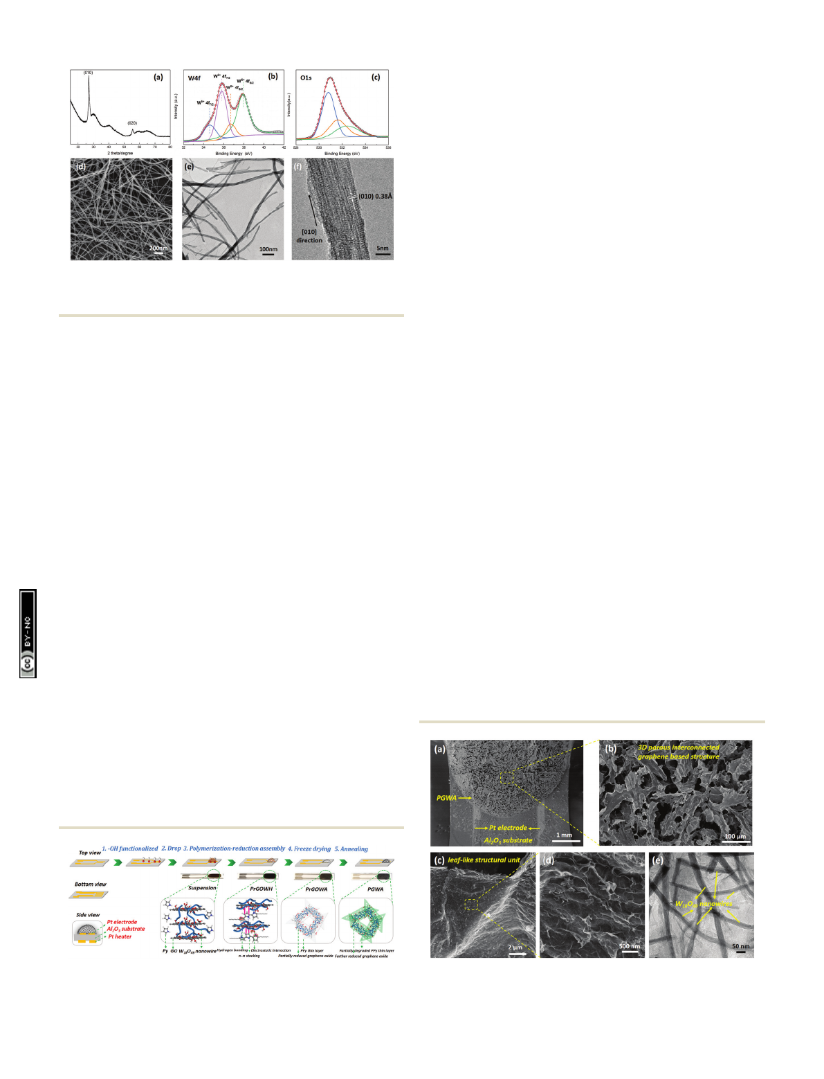
method. Fig. 1a shows the XRD pattern of the as-prepared
W
18
O
49
nanowires. The narrow (010) and (020) reflections indi-
cate that the crystal growth direction of W
18
O
49
nanowires is
[010].
14
The high-resolution W4f spectrum can be deconvoluted
into two doublets, which correspond to W
6+
and W
5+
oxidation
states (Fig. 1b). The dominant peaks at 530.7 eV, 531.5 eV and
533.2 eV in the O 1s XPS spectra (Fig. 1c) represent the oxygen
bond of W–O–W, oxygen vacancies and the adsorbed oxygen
species,
15
respectively.
Fachgebiet Keramische Werkstoffe/Chair of Advanced Ceramic Materials,
Technische Universita
¨t Berlin, Hardenbergstr. 40, 10623, Berlin, Germany.
†Electronic supplementary information (ESI) available. See DOI: 10.1039/
c9cc09092d
Received 22nd November 2019,
Accepted 29th November 2019
DOI: 10.1039/c9cc09092d
rsc.li/chemcomm
ChemComm
COMMUNICATION
Open Access Article. Published on 29 November 2019. Downloaded on 6/13/2020 9:21:05 PM.
This article is licensed under a
Creative Commons Attribution-NonCommercial 3.0 Unported Licence.
View Article Online
View Journal
| View Issue
This journal is ©The Royal Society of Chemistry 2020 Chem. Commun., 2020, 56, 450--453 | 451
As shown in Fig. 1d and e, the as-grown W
18
O
49
is comprised
of entangled nanowires with an average length of several micro-
meters and width of 10–20 nm. The wires are single-crystalline in
nature, confirmed by HRTEM (Fig. 1f). Clear lattice fringes with a
d-spacing of 0.38 nm can be discerned, corresponding to the
(010) planes of monoclinic W
18
O
49
.
16
This implies preferential
growth in the [010] direction, consistent with XRD observations.
Fig. 2 illustrates an in situ fabrication process of PPy coupled
graphene/W
18
O
49
nanowire aerogels (PGWAs) on a chip (a Al
2
O
3
substrate integrated with a Pt electrode on the positive side and a
Pt heater on the negative side). First, the substrate was hydroxyl
functionalized by Piranha solution in order to increase the bond-
ing strength between GO based solution and the substrate with
hydrogen bonding. GO aqueous suspension and pre-synthesized
W
18
O
49
nanowires were mixed together by ultrasonication, and
then a reducing agent, a conductive polymer monomer, Py, was
introduced (Fig. S2, ESI†). After that, W
18
O
49
nanowire containing
Py/GO suspension was dropped on the chip by a syringe with a
fine needle, followed by a polymerization–reduction process to
functionalize it and initiate sheet assembly into a 3D network.
After freeze-drying, the solvent was removed from the hydrogel to
produce polypyrrole coupled reduced graphene oxide/W
18
O
49
nanowire aerogels (PrGOWAs). After the further annealing process,
PGWAs were successfully integrated on a chip.
The direct on chip deposition is explained as follows. The GO
sheet is hydrophilic mainly due to the ionizable –COOH groups
at edges, while its basal plane is essentially hydrophobic due to a
network of polyaromatic islands of unoxidized benzene rings.
Therefore, the GO sheet can be considered as a surfactant with a
largely hydrophobic basal plane and hydrophilic edge, and
as a result, it would have the capability to disperse other nano-
materials in water homogeneously.
17
In this case, the GO sheets
support and prevent insoluble W
18
O
49
nanowires from precipita-
tion, forming stable suspensions. The Py monomer has a typical
conjugated structure with an electron-rich N atom, which may
easily attach on the surfaces and galleries of GO sheets through
hydrogen bonding, p–pstacking and electrostatic interaction,
18
coupling W
18
O
49
nanowires on graphene sheets simultaneously.
Therefore, the existence of Py will effectively prevent the self-
stacked behavior of GO during the reducing process, and
accordingly increase the available GO sheets for forming a
large volume of 3D graphene aerogels. A further annealing
process was utilized for further reduction of GO and partial
degradation of PPy, improving electrical contact and providing
more chemisorption sites to enhance the response.
Fig. 3(a–d) show the SEM images of the PGWA on the Al
2
O
3
substrate interdigitated Pt electrodes. They present the features
of tight adhesion between the PGWA and the device (Fig. 3(a))
and a highly porous structure with interconnected pores ranging
from tens to hundreds of micrometers (Fig. 3(b)), which endows
the sensing materials with low electrical resistance (Fig. S3, ESI†)
and a high specific surface area of 396 m
2
g
1
(Fig. S4, ESI†). In
contrast to the smooth surface of graphene sheets, the W
18
O
49
nanowires are randomly decorated on the micrometer sized
graphene sheet walls of the network (Fig. 3(c–e)), which are
coupled by a PPy thin layer in the PGWA. Furthermore, the
structure could be vividly described as a leaf tissue-like structure:
PPy is the epi-dermis, W
18
O
49
nanowires are the leaf veins and
graphene sheets are the mesophyll. For bare N-doped graphene
aerogels, even when the annealing temperature reaches 900 1C,
the aerogels still show robust adhesion on the device with typical
3D interconnected porous structures (Fig. S5, ESI†). It is evident
that this method is suitable for in situ assembly heteroatom-doped/
defective graphene aerogels and nanomaterial functionalized
graphene aerogels, which need post-treatment processes, such
as high temperature annealing or plasma treatment.
Fig. 1 (a) XRD pattern of W
18
O
49
nanowires, (b and c) W4f and O1s XPS
spectra, (d) SEM and (e) TEM images of W
18
O
49
nanowires, and (f) HRTEM
image of a single W
18
O
49
nanowire.
Fig. 2 Schematic illustration of the in situ fabrication process of 3D
graphene based aerogels on a chip.
Fig. 3 (a–d) SEM images of the PGWA on a chip at different magnifications
and (e) TEM image of the PGWA.
Communication ChemComm
Open Access Article. Published on 29 November 2019. Downloaded on 6/13/2020 9:21:05 PM.
This article is licensed under a
Creative Commons Attribution-NonCommercial 3.0 Unported Licence.
View Article Online
452 |Chem. Commun., 2020, 56, 450--453 This journal is ©The Royal Society of Chemistry 2020
To confirm the interaction between PPy and graphene after
the polymerization–reduction process, the ATR-FTIR spectra of
GO and graphene based aerogels are shown in Fig. S6 and S7
(ESI†). It can be found that the bonds related to the CQO,
C–OH and C–O groups of GO almost disappear, indicating the
efficient reduction of GO. The strong band around 1564 cm
1
is
attributed to typical ring vibrations of PPy,
19
andthatat1196cm
1
is due to the C–N stretching.
20
The band at 1041 cm
1
corre-
sponds to the C–H band in plane vibrations, suggesting
that PPy was indeed loaded onto the surface of graphene
throughinteractionssuchashydrogenbondingandp–pstacking
between them.
19,21
After the introduction of W
18
O
49
nanowires,
peaks at 787 and 715 cm
1
are observed, which are assigned to
O–W–O stretching modes. The bands centered at 655 and
585 cm
1
are attributed to the W–O–W stretching modes.
22
The
partial characteristic peaks assigned to C–H in-plane and out-of-
plane vibrations at 1041 cm
1
and 916 cm
1
of the PPy diminished
after the annealing treatment, and no new characteristic peaks were
observed, showing the degradation of the polymer. Furthermore, the
chemical states of PGWAs are investigated by XPS (Fig. S8, ESI†). The
initial GO is well reduced to graphene by polymerization–
reduction and annealing processes, confirmed by significantly
improving the intensity of sp
2
C–C bonds of graphene at 284.6 eV
and decreasing the oxygen containing carbon (epoxy C–O at
286.6 eV, carbonyl CQO at 287.6 eV, and carboxyl O–CQOat
288.9 eV), as analyzed from the corresponding deconvolution of
the C1s spectra of the as-prepared aerogels and GO (Fig. S9 and
S10, ESI†). It should be noticed that the PGWA exhibits a nitrogen
contentof4.26at%afterannealing(TableS1,ESI†). Besides, the
high resolution N1s spectrum of the PGWA could be fitted well
with three different signals corresponding to pyridinic N, pyrrolic
N, and graphitic N, respectively (Fig. S11, ESI†), which further
confirms PPy functionalization on the surfaces of graphene and N
atoms doped in graphene. Further investigation of the phase
evolution of GO is characterized by XRD. As shown in Fig. S12(a)
(ESI†), the (001) crystal plane of GO was evident, with an interlayer
spacingof8.33Å.Afterthepolymerization–reduction process, the
PGA showed a broad reflection at 2y=261(Fig. S12(b), ESI†),
which is typical of reduced GO materials. The nanowires still
exhibit the feature of a monoclinic crystal phase of W
18
O
49
after
the further annealing process.
Based on all these findings, we can conclude that our fabrica-
tion procedure is suitable for the incorporation of 3D based
graphene aerogels into electronic devices. As a proof-of-concept,
the as-fabricated 3D graphene based aerogels are directly used as
a gas sensor for the detection of low concentrations of NO
2
gas.
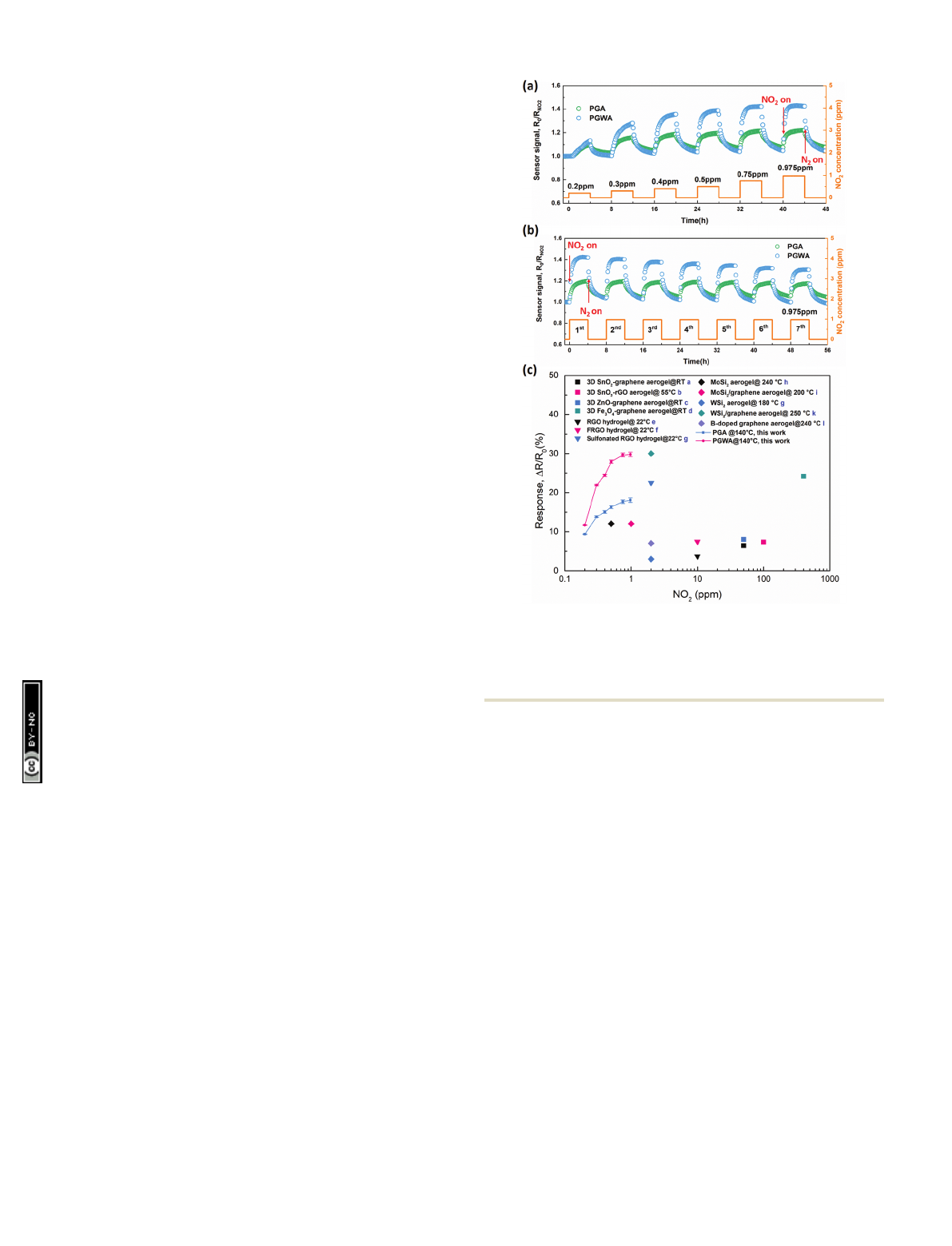
Fig. 4a shows the time dependent response of the graphene
based aerogel sensors to various NO
2
concentrations, from 200
to 975 ppb, with an operating temperature of 140 1C (Fig. S13,
ESI†), which represents an optimum for the sensor signal and
response/recovery time. At low temperature, the adsorption of
NO
2
is substantial and continues during gas exposure, while its
desorption is negligible due to the strong bonding between NO
2
and the PGA as well as the PGWA. The NO
2
desorption is
enhanced at higher temperature, which speeds up the time to
reach a balance between adsorption and desorption both during
gas exposure and during recovery. Although the response and
recovery times might be even faster at higher temperature, 140 1C
is considered an effective temperature when also considering the
sensor signal.
Upon exposure to NO
2
at 140 1C, the PGWA sensor presents
higher response (DR/R
0
= 29.78%) towards 0.975 ppm of NO
2
gas
compared to the PGA sensor (DR/R
0
= 18.04%) demonstrating the
remarkably improved response achieved by functionalization
with W
18
O
49
nanowires. Furthermore, to investigate the repeat-
ability and stability of aerogel based sensors, the PGA and PGWA
sensors were exposed to 0.975 ppm of NO
2
for seven successive
cycles. An average response (DR/R
0
= 25.4%) of the PGWA sensor
with a small standard deviation of 1.9% is measured (Fig. 4b),
verifying the reliable repeatability of the sensors. Moreover,
compared with the gas sensing performance of graphene-based
aerogels by the traditional deposition method (Fig. S14, ESI†),
the PGWA assembled on a chip not only shows higher response,
but also presents low noise of the sensor signal originating from
its low electrical resistance (Fig. S15, ESI†).
Fig. 4(c) displays sensor response to NO
2
above 200 ppb,
displaying a nonlinear relationship between the sensor
response (DR/R
0
) and gas concentration, which is typical for
Fig. 4 (a) Transient sensor response at 140 1C towards different NO
2
con-
centrations. (b) Reproducibility of sensor response exposed to 0.975 ppm NO
2
at 140 1C. (c) Comparison with reported graphene based aerogels/hydrogels
at optimized temperatures for NO
2
sensors (a,
24
b,
9
c,
25
d,
26
e,
11a
f,
8a
g,
7c
h,
27
i,
7b
j,
28
k,
10c
l,
10b
).
ChemComm Communication
Open Access Article. Published on 29 November 2019. Downloaded on 6/13/2020 9:21:05 PM.
This article is licensed under a
Creative Commons Attribution-NonCommercial 3.0 Unported Licence.
View Article Online
This journal is ©The Royal Society of Chemistry 2020 Chem. Commun., 2020, 56, 450--453 | 453
chemiresistive sensors.
23
Assuming that the gas adsorption is
dominated by high-energy defect sites, at low NO
2
concentra-
tions when most of the sites are available, the charge transfer is
directly proportional to the gas concentration. At higher NO
2
concentrations, all sites may eventually be occupied during the
gas exposure, and thus the response reaches a saturation point.
To highlight the high sensing performance of the PGWA sensor
fabricated in this work, the response of reported graphene based
aerogels/hydrogels and two-dimensional metal sulfide aerogels are
summarized in Fig. 4(c), which demonstrated the outstanding
response towards low concentrations of NO
2
gas.
The sensing performance of the in situ assembled 3D graphene
based aerogels results from: (a) high conductivity of 3D intercon-
nected graphene aerogels necessary for efficient operation of the
sensors, (b) a highly porous structure with a high surface area
that provides a large number of surface active sites necessary for
the reliable detection of low NO
2
concentrations, and (c) hetero-
junctions between n-type W
18
O
49
nanowires and p-type graphene
as well as p-type PPy which is beneficial for enhancing gas
sensitivity in chemiresistors.
In conclusion, we have successfully in situ assembled 3D
interconnected porous PPy coupled graphene/W
18
O
49
nanowire
aerogels on a chip by a polymerization–reduction route followed
by an annealing process. Py initiates and mediates the assembly
of GO sheets and W
18
O
49
nanowires into a 3D network in a facile,
environment-friendly and scalable route. As a proof of concept,
the as-fabricated 3D graphene based aerogels are applied as gas
sensors for the detection of low concentrations of NO
2
gas. The
strategy developed here allows for direct integration of graphene
based aerogels into functional devices and opens up new per-
spectives for the fabrication of functional devices.
Conflicts of interest
There are no conflicts to declare.
Notes and references
1 J. Mao, J. Iocozzia, J. Huang, K. Meng, Y. Lai and Z. Lin, Energy
Environ. Sci., 2018, 11, 772–799.
2 N. Yousefi, X. Lu, M. Elimelech and N. Tufenkji, Nat. Nanotechnol.,
2019, 14, 107–119.
3 B. Qiu, M. Xing and J. Zhang, Chem. Soc. Rev., 2018, 47, 2165–2216.
4 T. T. Tung, M. J. Nine, M. Krebsz, T. Pasinszki, C. J. Coghlan,
D. N. H. Tran and D. Losic, Adv. Funct. Mater., 2017, 27, 1702891.
5 S. S. Varghese, S. Lonkar, K. K. Singh, S. Swaminathan and
A. Abdala, Sens. Actuators, B, 2015, 218, 160–183.
6 Y. H. Zhang, Y. B. Chen, K. G. Zhou, C. H. Liu, J. Zeng, H. L. Zhang
and Y. Peng, Nanotechnology, 2009, 20.
7(a) A. Harley-Trochimczyk, T. Pham, J. Chang, E. Chen, M. A.
Worsley, A. Zettl, W. Mickelson and R. Maboudian, Adv. Funct.
Mater., 2016, 26, 433–439; (b) H. Long, A. Harley-Trochimczyk,
T. Pham, Z. R. Tang, T. L. Shi, A. Zettl, C. Carraro, M. A. Worsley
and R. Maboudian, Adv. Funct. Mater., 2016, 26, 5158–5165; (c) J. Wu,
K. Tao, Y. Guo, Z. Li, X. Wang, Z. Luo, S. Feng, C. Du, D. Chen,
J. Miao and L. K. Norford, Adv. Sci., 2017, 4, 1600319.
8(a) J. Wu, K. Tao, J. Zhang, Y. Guo, J. Miao and L. K. Norford,
J. Mater. Chem. A, 2016, 4, 8130–8140; (b) T. Alizadeh and
F. Ahmadian, Anal. Chim. Acta, 2015, 897, 87–95.
9 L. Li, S. J. He, M. M. Liu, C. M. Zhang and W. Chen, Anal. Chem.,
2015, 87, 1638–1645.
10 (a) D. M. Guo, P. J. Cai, J. Sun, W. N. He, X. H. Wu, T. Zhang,
X. Wang and X. T. Zhang, Carbon, 2016, 99, 571–578; (b) S. Turner,
W. Yan, H. Long, A. J. Nelson, A. Baker, J. R. I. Lee, C. Carraro,
M. A. Worsley, R. Maboudian and A. Zettl, J. Phys. Chem. C,
2018, 122, 20358–20365; (c) W. Yan, M. A. Worsley, T. Pham,
A. Zettl, C. Carraro and R. Maboudian, Appl. Surf. Sci., 2018, 450,
372–379.
11 (a) J. Wu, K. Tao, J. Miao and L. K. Norford, ACS Appl. Mater.
Interfaces, 2015, 7, 27502–27510; (b) N. H. Ha, D. D. Thinh,
N. T. Huong, N. H. Phuong, P. D. Thach and H. S. Hong, Appl. Surf.
Sci., 2018, 434, 1048–1054.
12 (a) M. Graf, A. Gurlo, N. Ba
ˆrsan, U. Weimar and A. Hierlemann,
J. Nanopart. Res., 2006, 8, 823–839; (b)L.Ma
¨dler, A. Roessler,
S. E. Pratsinis, T. Sahm, A. Gurlo, N. Barsan and U. Weimar, Sens.
Actuators, B, 2006, 114, 283–295.
13 J. Polleux, A. Gurlo, N. Barsan, U. Weimar, M. Antonietti and
M. Niederberger, Angew. Chem., 2006, 118, 267–271.
14 (a)G.Xi,S.Ouyang,P.Li,J.Ye,Q.Ma,N.Su,H.BaiandC.Wang,Angew.
Chem., Int. Ed., 2012, 51, 2395–2399; (b)W.Cheng,Y.Ju,P.Payamyar,
D. Primc, J. Rao, C. Willa, D. Koziej and M. Niederberger, Angew. Chem.,
Int. Ed., 2015, 54, 340–344.
15 X. Zhong, Y. Sun, X. Chen, G. Zhuang, X. Li and J.-G. Wang, Adv.
Funct. Mater., 2016, 26, 5778–5786.
16 Y. Tian, S. Cong, W. Su, H. Chen, Q. Li, F. Geng and Z. Zhao, Nano
Lett., 2014, 14, 2150–2156.
17 (a) Z. Niu, L. Liu, L. Zhang, Q. Shao, W. Zhou, X. Chen and S. Xie,
Adv. Mater., 2014, 26, 3681–3687; (b) S. Hu, T. Han, C. Lin, W. Xiang,
Y. Zhao, P. Gao, F. Du, X. Li and Y. Sun, Adv. Funct. Mater., 2017,
27, 1700041.
18 Y. Zhao, J. Liu, Y. Hu, H. Cheng, C. Hu, C. Jiang, L. Jiang, A. Cao and
L. Qu, Adv. Mater., 2013, 25, 591–595.
19 J. Sun, X. Shu, Y. Tian, Z. Tong, S. Bai, R. Luo, D. Li and C. C. Liu,
Sens. Actuators, B, 2017, 241, 658–664.
20 X. Chen, J. Chen, F. Meng, L. Shan, M. Jiang, X. Xu, J. Lu, Y. Wang
and Z. Zhou, Compos. Sci. Technol., 2016, 127, 71–78.
21 Z. Fan, J. Zhu, X. Sun, Z. Cheng, Y. Liu and Y. Wang, ACS Appl.
Mater. Interfaces, 2017, 9, 21763–21772.
22 (a) Y. Qin, T. Zhang and Z. Cui, Org. Electron., 2017, 48, 254–261;
(b) B. Bhuyan, B. Paul, S. S. Dhar and S. Vadivel, Mater. Chem. Phys.,
2017, 188, 1–7.
23 A. Gurlo, Nanoscale, 2011, 3, 154–165.
24 X. Liu, J. S. Cui, J. B. Sun and X. T. Zhang, RSC Adv., 2014, 4,
22601–22605.
25 X. Liu, J. B. Sun and X. T. Zhang, Sens. Actuators, B, 2015, 211,
220–226.
26 X. Liu, J. W. Li, J. B. Sun and X. T. Zhang, RSC Adv., 2015, 5,
73699–73704.
27 H. Long, L. Chan, A. Harley-Trochimczyk, L. E. Luna, Z. Tang, T. Shi,
A. Zettl, C. Carraro, M. A. Worsley and R. Maboudian, Adv. Mater.
Interfaces, 2017, 4, 1700217.
28 W. Yan, A. Harley-Trochimczyk, H. Long, L. Chen, T. Pham, M. Hu,
Y. Qin, A. Zettl, C. Carraro, M. A. Worsley and R. Maboudian,
FlatChem, 2017, 5, 1–8.
Communication ChemComm
Open Access Article. Published on 29 November 2019. Downloaded on 6/13/2020 9:21:05 PM.
This article is licensed under a
Creative Commons Attribution-NonCommercial 3.0 Unported Licence.
View Article Online
Loading more pages...