
Radiative Recombination and Carrier Injection Efficiencies
in 265 nm Deep Ultraviolet Light-Emitting Diodes Grown
on AlN/Sapphire Templates with Different Defect
Densities
Anton Muhin,* Martin Guttmann, Verena Montag, Norman Susilo, Eviathar Ziffer,
Luca Sulmoni, Sylvia Hagedorn, Neysha Lobo-Ploch, Jens Rass, Leonardo Cancellara,
Shaojun Wu, Tim Wernicke, and Michael Kneissl
1. Introduction
AlGaN-based deep ultraviolet light-
emitting diodes (DUV LEDs) with emis-
sion wavelengths shorter than 280 nm
have multiple applications ranging from
disinfection of surfaces
[1–3]
and virus
inactivation
[4–6]
to chemical and biochemi-
cal sensing.
[7,8]
Nevertheless, the external
quantum efficiency (ηEQE) of these devices
remains far below the values reached by
blue LEDs.
[9–11]
In fact, due to several draw-
backs, the ηEQE, which consists of the
radiative recombination efficiency (ηRRE),
the carrier injection efficiency (ηCIE), and
the light extraction efficiency (ηLEE),
decreases drastically at shorter
wavelengths.
[9–13]
The ηLEE is the most lim-
iting factor to the efficiency of DUV
LEDs.
[10,14]
The outcoupling of photons
emitted by radiatively recombined charge
carriers becomes increasingly difficult with
increasing Al mole fraction in the multiple
quantum well (MQW) regions due to
transverse-magnetic polarized emission
emerging as dominant over the transverse-electric polarized
emission.
[15–17]
Since it is very difficult to overcome this
A. Muhin, M. Guttmann, V. Montag, E. Ziffer, L. Sulmoni, S. Wu,
T. Wernicke, M. Kneissl
Institute of Solid State Physics
Technische Universität Berlin
Hardenbergstraße 36, 10623 Berlin, Germany
E-mail: anton.muhin@tu-berlin.de
The ORCID identification number(s) for the author(s) of this article
can be found under https://doi.org/10.1002/pssa.202200458.
© 2022 The Authors. physica status solidi (a) applications and materials
science published by Wiley-VCH GmbH. This is an open access article
under the terms of the Creative Commons Attribution-NonCommercial-
NoDerivs License, which permits use and distribution in any medium,
provided the original work is properly cited, the use is non-commercial
and no modifications or adaptations are made.
DOI: 10.1002/pssa.202200458
M. Guttmann, S. Hagedorn, N. Lobo-Ploch, J. Rass
Ferdinand-Braun-Institut (FBH)
Gustav-Kirchhoff-Straße 4, 12489 Berlin, Germany
L. Cancellara
Leibniz-Institut für Kristallzüchtung (IKZ)
Max-Born-Str. 2, 12489 Berlin, Germany
The electro-optical characteristics of deep ultraviolet light-emitting diodes (DUV
LEDs) emitting at 265 nm and grown on AlN/sapphire templates with different
threading dislocation densities, i.e., high-temperature annealed (HTA) AlN, epitax-
ially laterally overgrown (ELO) AlN, and HTA-ELO AlN are analyzed. The external
quantum efficiency of each individual device is separated into maximum radiative
recombination efficiency, carrier injection efficiency, and light extraction efficiency.
This is achieved by combining an ABC-model-based fit of the current-dependent
external quantum efficiency together with calibrated Monte Carlo ray-tracing sim-
ulations. A maximum radiative recombination efficiency between 50% and 60% is
estimated for DUV LEDs grown on ELO and HTA-ELO AlN/sapphire, whereas the
values for devices grown on HTA AlN/sapphire are around 45%. The extracted
radiative recombination efficiency does not scale with the measured threading
dislocation density (TDD), even when accounting for the inhomogeneous TDD in the
AlN base layers. This discrepancy is attributed to the formation of dislocation half-
loops introduced by additional compressive strain caused by the HTA process and
mayresultintheformationofadditionalnonradiative recombination centers in the
AlGaN multi-quantum well region. In addition, the carrier injection efficiency values
ranging from 45% to 55% are determined for devices grown on all three templates.
RESEARCH ARTICLE
www.pss-a.com
Phys. Status Solidi A 2023,220, 2200458 2200458 (1 of 7) © 2022 The Authors. physica status solidi (a) applications and materials science
published by Wiley-VCH GmbH

fundamental material property, present research mainly focuses
on increasing ηRRE and ηCIE. However, the determination of abso-
lute values for both these quantities, especially separately and
under electrical injection, is not straightforward. Therefore, some
of the most exigent questions regarding the performance of DUV
LEDs are still under debate, e.g., how strongly and to which extent
the individual crystal defects, i.e., threading dislocations (TD)
and point defects affect the ηRRE.
[18,19]
Additionally, despite the
consensus about the decrease in ηCIE with shorter emission wave-
lengths,
[12]
reports on the quantitative ηCIE values for DUV LEDs
are rare. In addition to the simulation results, most publications
discussing the ηCIE of DUV LEDs limit the analysis to a compari-
son of device performance with different carrier confinement and
electron blocking concepts.
[20–22]
Thus, reliable values for ηRRE and
ηCIE are required in order to identify the key aspects with the high-
est potential for further optimization of DUV LEDs. In this article,
DUV LEDs grown on three types of templates with different
threading dislocation densities (TDDs) are analyzed and com-
pared. The ηLEE and the ηRRE were extracted from Monte Carlo
ray-tracing simulations and from the generalized ABC model
fit of the current dependent ηEQE, respectively. This way, it was
then possible to derive the carrier injection efficiency from the
measured external quantum efficiency.
2. Experimental Section
AlGaN-based DUV LEDs with an emission wavelength of
265 nm were grown side by side in one growth run by
metal–organic vapor phase epitaxy (MOVPE) on three different
templates: high-temperature annealed (HTA) AlN/sapphire, epi-
taxially laterally overgrown (ELO) AlN/sapphire, and HTA-ELO
AlN/sapphire, as shown in Figure 1. These templates were over-
grown with an AlN buffer and a Si-doped n-AlGaN current
spreading layer followed by a threefold Al
0.62
Ga
0.38
N/
Al
0.48
Ga
0.52
N MQW, an electron blocking layer (EBL) consisting
of a 10 nm thick undoped Al
0.85
Ga
0.15
N and a 25 nm thick
Al
0.75
Ga
0.25
N:Mg layer, capped by a 200 nm thick GaN:Mg con-
tact layer. To analyze the defect densities in the AlGaN MQW
regions, samples with identical heterostructure to the DUV
LEDs without p-side and with a thicker last AlGaN barrier
(40 nm) were grown on the three different templates. Further
details on the heterostructure, growth conditions, and template
fabrication process are reported in reference.
[23]
After thermal
activation of Mg acceptors, the DUV LEDs were fabricated simul-
taneously by standard micro-fabrication techniques using Pd/Au
p-contacts and V/Al/Ni/Au n-contacts.
[24]
All relevant device
characteristics are summarized in Table 1.
The ηLEE for the DUV LEDs was calculated by Monte Carlo ray-
tracing simulations taking into account the degree of polarization
of the MQW emission as well as far-field measurements.
[25]
The light extraction efficiency of the DUV LEDs grown on
ELO and HTA-ELO template was found to be similar with
6.8% 0.7% and 6.7% 0.7%, respectively, whereas the ηLEE
value for devices grown on the HTA template is slightly lower
with 6.1% 0.6%. This is attributed to light scattering at the
air voids in the ELO structure and thus a change in the angular
distribution of the light at the sapphire–air interface.
The TDD within the AlN base layers and the MQW regions
was estimated by high-resolution X-ray diffraction (HR-XRD),
cross-sectional transmission electron microscopy (TEM) diffrac-
tion, and plane-view panchromatic cathodoluminescence
(CL) on the AlGaN MQW samples. All three methods showed
comparable results, i.e., the dark spot density (DSD) from the
CL measurements, which is assumed to be identical to the
TDD,
[19]
has the lowest value for the MQW structure grown
on the HTA-ELO AlN/sapphire (0.95 0.1 10
9
cm
2
),
followed by the sample grown on HTA AlN/sapphire
(1.1 0.05 10
9
cm
2
) and by ELO AlN/sapphire
(1.6 0.2 10
9
cm
2
).
[23]
The electro-optical on-wafer measurements of the DUV LEDs
were carried out in continuous wave mode up to current
densities j<1Acm
2
using a picoammeter (Keithley 6487).
Measurements for higher current densities were performed in
pulsed mode (Avtech, AV-1010-B) with a pulse width (t
pulse
)of
5μs and a duty cycle of 1% using a current probe and a digitizing
oscilloscope (Tektronix, TDS 2024B). This combined procedure
enables us to resolve low current densities and to reduce the
Joule heating at higher j. The negligible influence of the pn junc-
tion heating during the pulsed operation was verified by applying
lower duty cycles and shorter pulses, resulting in identical DUV
LED characteristics.
Figure 1. Templates used in this work: high-temperature annealed (HTA) AlN/sapphire (left), epitaxially laterally overgrown (ELO) AlN/sapphire (center),
and HTA-ELO AlN/sapphire (right).
Table 1. Summary of the device characteristics. All values except ηLEE
represent average values over all devices grown on a specific template.
AlN/sapphire
template
Specification DSD 10
9
[cm
2
]
ηEQE
max
[%]
ηLEE [%] ηIQE
max
[%]
ηRRE
max
[%]
ηCIE
[%]
ELO on-wafer 1.6 0.2 1.7 6.8 0.7 25 57 45
HTA on-wafer 1.1 0.05 1.4 6.1 0.6 23 45 51
HTA-ELO on-wafer 0.95 0.1 1.8 6.7 0.7 27 58 46
HTA-ELO mounted 0.95 0.1 2.6 9.2 0.9 30 60 52
HTA-ELO mounted and
encapsulated
0.95 0.1 4.7 12.8 1.3 35 60 58
www.advancedsciencenews.com www.pss-a.com
Phys. Status Solidi A 2023,220, 2200458 2200458 (2 of 7) © 2022 The Authors. physica status solidi (a) applications and materials science
published by Wiley-VCH GmbH
3. Data Processing
For the determination of the radiative recombination efficiency,
an ABC-model-based method introduced by Titkov et al.
[26]
was
utilized. According to the ABC model, the ηEQE of an LED is
given by
ηEQE ¼ηLEEηCIEηRRE ¼ηLEEηCIE Bn
AþBn þCn2(1)
where nis the charge carrier concentration, while A,B, and Care
constants corresponding to the Shockley–Read–Hall (SRH) non-
radiative recombination, the bimolecular radiative recombina-
tion, and the non-radiative Auger recombination, respectively.
Using the normalized optical power p¼Pout=Pmax, where Pout
is the measured optical output power and Pmax is the optical
output power at the peak external quantum efficiency ηEQE
max ,
the following relation can be derived from the ABC model
[27]
ηRRE ¼Q
Qþp1=2þp1=2(2)
where Qis a dimensionless parameter called “quality factor,”
which is directly related to the peak radiative recombination effi-
ciency: ηRRE
max ¼Q
Qþ2. Thus, it follows
ηEQE
max
ηEQE ¼ηRRE
max
ηRRE ¼ηRRE
max þp1=2þp1=2
Qþ2(3)
By plotting ηEQE
max /ηEQE versus p1=2þp1=2and fitting the data
points by a linear function, Qand therefore ηRRE
max can be directly
evaluated from the slope of the fitting line. However, the
described relations are only valid if ηLEE and ηCIE are current
(I) independent. It is fairly safe to assume that the light extraction
efficiency is independent of the drive current, since its value
mostly depends on the refractive index values of the heterostruc-
ture layers.
[28]
To satisfy the constant ηCIEðIÞcondition, the linear
fitting of data points in the ηEQE
max /ηEQE versus p1=2þp1=2plots
was carried out only for values around ηEQE
max . This narrow fitting
range corresponds to current densities between 0.6 and
60 A cm
2
and ensures only minor changes in ηCIEðIÞ. Any devi-
ations from ηCIEðIÞor ηLEEðIÞbeing constant or from the ABC
model itself lead to a nonlinear behavior in the ηEQE
max /ηEQE versus
p1=2þp1=2plots and are considered in the evaluation by an
increased fitting error.
[28]
Finally, as a result of the simulated
ηLEE and the extracted ηRRE
max values, ηCIE is calculated by using
Equation (1).
4. Results and Discussion
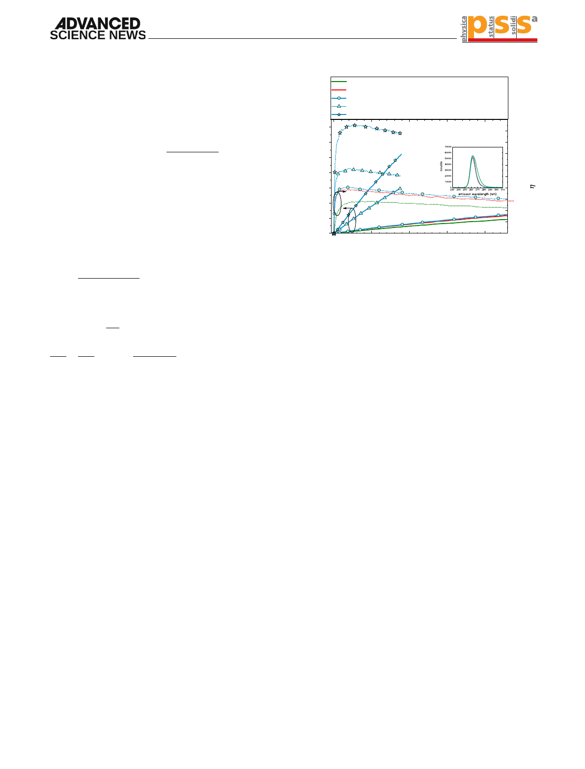
The measured electro-optical characteristics of typical
unmounted DUV LEDs grown on different templates are shown
in Figure 2. The highest optical output power of 12.3 mW at
100 A cm
2
is achieved for devices grown on HTA-ELO AlN/
sapphire, having a maximum external quantum efficiency of
1.9%. DUV LEDs grown on ELO AlN/sapphire exhibit a
slightly lower performance: Pout ¼11.6 mW at 100 A cm
2
and
ηEQE
max ¼1.8%. The lowest optical output power of
Pout ¼9.2 mW at 100 A cm
2
and ηEQE
max ¼1.4% is reached by devi-
ces grown on HTA AlN/sapphire templates. Both Pout and ηEQE
max
do not follow the TDD trend for the individual AlN base layers
and the AlGaN MQW region, as shown in Table 1. This is unex-
pected, as one would anticipate the TDD to have a major impact
on the ηRRE and thus on the LED performance due to changes in
non-radiative SRH recombination rates.
[29]
To eliminate the
influence of the different light extraction efficiencies, which
might explain the aforementioned disagreement, the peak inter-
nal quantum efficiencies ηIQE
max ¼ηRRE
max ηCIE are determined by
dividing the measured ηEQE
max by the simulated ηLEE. In fact, among
all characterized devices the highest ηIQE
max around 28.5% is
reached by LEDs grown on the HTA-ELO AlN/sapphire, having
the lowest TDD. However, the average ηIQE
max of LEDs grown on the
HTA-ELO AlN/sapphire (27%) is similar to the one grown on the
ELO template (25%) despite the significant TDD difference of
more than 70%. Additionally, the ηIQE
max of the devices grown
on ELO AlN/sapphire is higher compared to that of LEDs
grown on the HTA AlN/sapphire (23%) in spite of the
higher TDD.
4.1. Determination of the Radiative Recombination Efficiency
To understand how the TDD influences solely the radiative
recombination efficiency, without the influence of the carrier
injection efficiency, the ηRRE is extracted from the electro-optical
device characteristics by applying the method described in
Section 3. An example of an ηEQE
max /ηEQE versus p1=2þp1=2plot
is shown in Figure 3a for an LED grown on HTA-ELO AlN/
sapphire. As it is indicated by the thick red line, the experimental
0 50 100 150 200
0
20
40
60
80
100
120
140
current density j (Acm-2)
optical output power P
out
(mW)
HTA AlN/sapphire
ELO AlN/sapphire
HTA ELO AlN/sapphire
HTA ELO AlN/sapphire (mounted)
HTA ELO AlN/sapphire (mounted and encapsulated)
0.0
0.5
1.0
1.5
2.0
2.5
3.0
3.5
4.0
4.5
5.0
Pulsed mode measurements
t
pulse
= 5 µs, duty cycle = 1%
T = RT
EQE
(%)
UVC-LED grown on top of:
Figure 2. Pout and ηEQE as a function of current density for representative
deep ultraviolet light-emitting diodes (DUV LEDs) grown on different AlN/
sapphire template measured in pulsed operation at room temperature
(RT). Additionally, characteristics of on-wafer, mounted, and encapsulated
LEDs grown on HTA-ELO AlN/sapphire are shown. The inset shows the
respective emission spectra.
www.advancedsciencenews.com www.pss-a.com
Phys. Status Solidi A 2023,220, 2200458 2200458 (3 of 7) © 2022 The Authors. physica status solidi (a) applications and materials science
published by Wiley-VCH GmbH
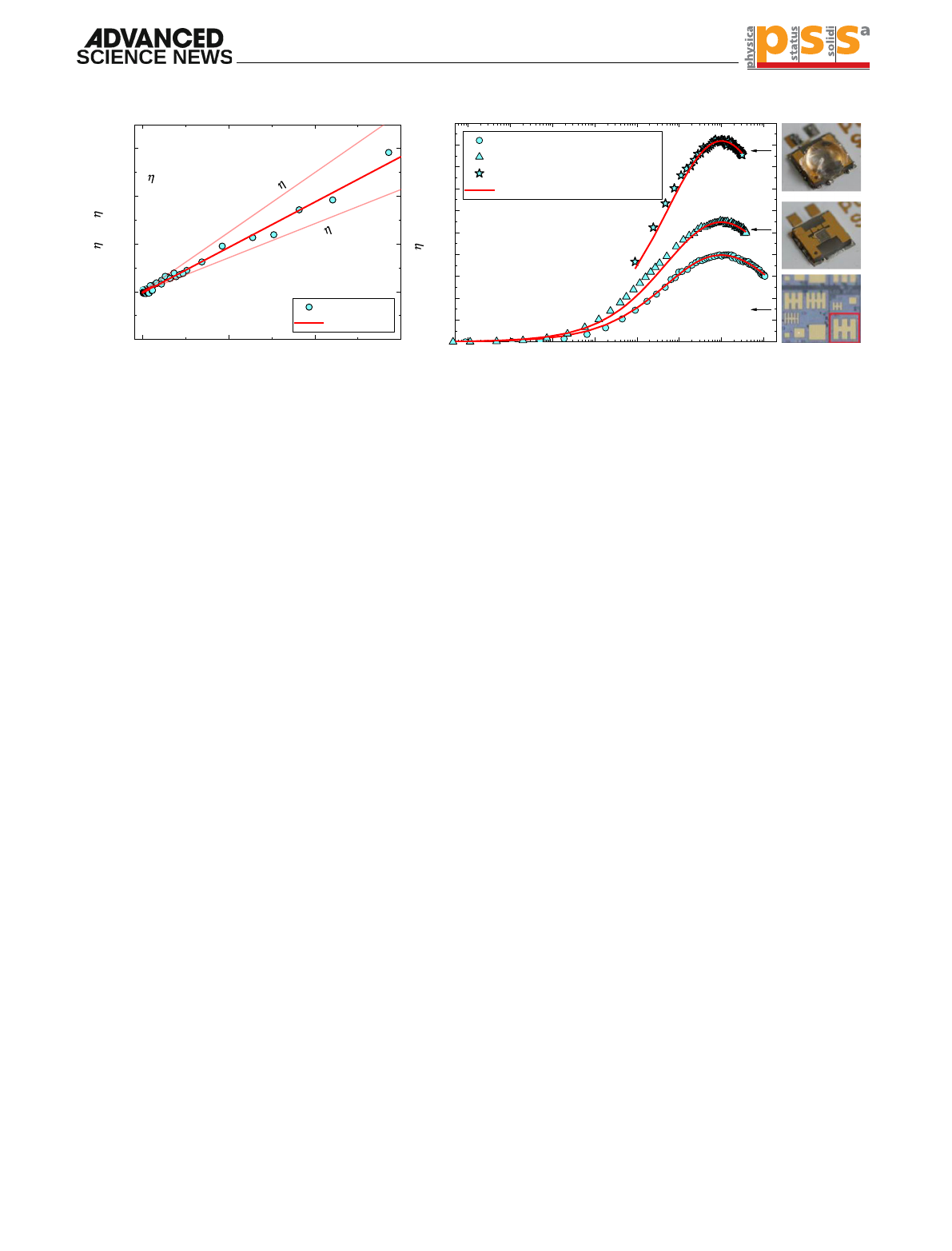
data points are in good agreement with a linear fit function allow-
ing for a reliable ηRRE
max estimation of 62 3% in this case.
Furthermore, Figure 3b shows the excellent fit of the measured
ηEQE dependence on the normalized optical output power from
Equation (2) obtained from the LED reported in Figure 3a. The
remarkable agreement over more than six orders of magnitude
justifies the previous assumption of ηCIE being only weakly
dependent on jwithin the fitting range. In addition, the robust-
ness of the method was validated by analyzing DUV LEDs grown
on HTA-ELO AlN/sapphire at different stages of the fabrication
process. For this purpose, the LEDs on the wafer were diced and
flip-chip mounted on AlN ceramic packages, as shown in
Figure 3d. The best performing device (ηIQE
max ¼35%) was then
encapsulated by a UV-transparent silicone resin “Deep
UV200,”
[30]
as shown inFigure 3e. The MQW region area (A)
of the mounted devices (A¼5.7 10
7
m
2
) differs from that
of DUV LEDs measured on-wafer (A¼1.5 10
7
m
2
). Also
the light extraction efficiency of mounted DUV LEDs
(ηLEE ¼9.2 0.9%) is higher compared to unmounted devices
(ηLEE ¼6.7 0.7%) due to packaging and increases further for
the encapsulated LED (ηLEE ¼12.8 1.3%). An emission power
of 103 mW at 90 A cm
2
was reached by the encapsulated LED
having a maximum external quantum efficiency of 4.7%. As it is
shown in Figure 3b, regardless of the different geometries and
light extraction efficiencies, the extracted ηRRE
max values of the rep-
resentative mounted LED with (ηRRE
max ¼58 4%) and without
encapsulation (ηRRE
max ¼60 3%) is almost equal to the one from
the on-wafer measurements. Furthermore, considering the sim-
ulated ηLEE and the extracted ηRRE
max values, the ηCIE was calculated
from the measured ηEQE
max by using Equation (1). Despite different
ηLEE values, the carrier injection efficiency for mounted and
unmounted devices is in the same range, between 45% and
55%. Only the ηCIE. of the encapsulated LED is with 58 8%
higher compared to other devices which is the reason for its out-
standing performance. In addition, the AlGaN MQW structure
grown on an ELO AlN/sapphire was analyzed by selective exci-
tation time-resolved photoluminescence (TRPL).
[31]
It was found
that at room temperature (RT) the ηRRE reaches values of
60% 10% and, as it will be shown next, is in line with the
ηRRE
max values extracted in this work. This agreement underlines
the reliability of the Titkov method for the given case.
Next, being confident about reproducibility and the absolute
values of the determined results, the influence of the template
on the radiative recombination efficiency can be discussed.
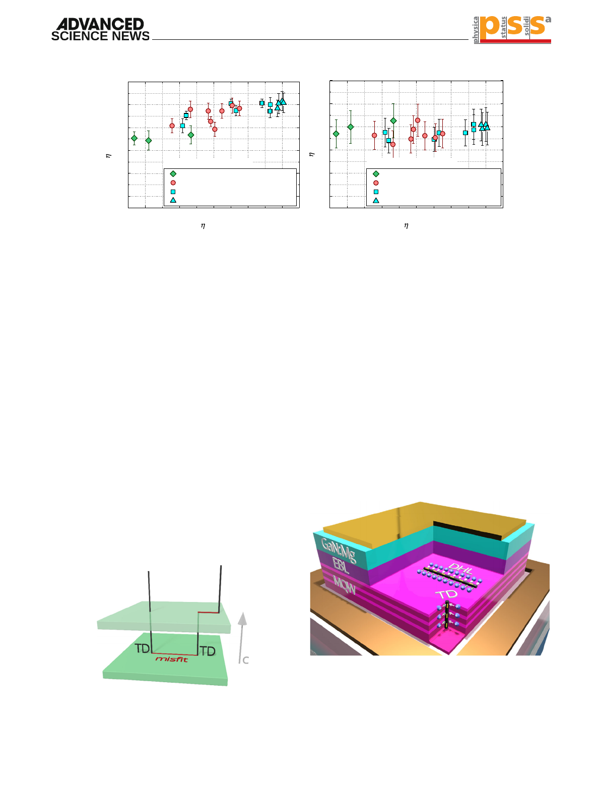
The extracted ηRRE
max values for all characterized devices are sum-
marized in Figure 4a. As is the case for external and internal
quantum efficiencies, the ηRRE
max of DUV LEDs grown on the
ELO and the HTA-ELO AlN/sapphire are in the same range
and vary between 50% and 60%. The values for DUV LEDs
grown on the HTA AlN/sapphire are lower and scatter around
45%. This suggests that the HTA step introduces additional non-
radiative recombination centers besides the TDs and therefore
reduces further the efficiency of devices grown on HTA and
HTA-ELO AlN/sapphire.
4.2. Influence of the HTA Process on
η
RRE
There are two critical impacts of the HTA process which can
impede the radiative recombination efficiency: the incorporation
of impurities and the increased compressive strain (ε) of AlN.
The incorporation of silicon, carbon, and oxygen into HTA-
AlN is a well-known side effect of the HTA step.
[32–35]
Indeed,
according to secondary ion mass spectrometry (SIMS) analysis,
O, C, and Si levels in the HTA-AlN are high and reach concen-
trations of 5 10
20
,410
18
, and 9 10
16
cm
3
, respectively
(shown in Supporting Information). However, there is no signif-
icant diffusion of these impurities from HTA-AlN into the AlN
base layers of the subsequently grown LED heterostructure. For
the investigated devices grown on the HTA AlN/sapphire tem-
plate, the MQW region is separated by almost 2 μm from the
2345
0.8
1.0
1.2
1.4
1.6
Q = 5
RRE
max
= 72%
EQE
max
/
EQE
p
1/2
+p
-1/2
experiment
ABC-fit
T = 300K
Q = 3.25 ± 0.25
RRE
max
= 62 ± 3%
Q = 2
RRE
max
= 50%
1E-6 1E-5 1E-4 1E-3 0.01 0.1 1 10
0.0
0.5
1.0
1.5
2.0
2.5
3.0
3.5
4.0
4.5
5.0
EQE
(%)
Normalized optical power p
on-wafer
mounted
mounted and encapsulated
ABC-fit
(a) (b)
(c)
(d)
(e)
Figure 3. a) ηEQE
max /ηEQE ratio as a function of p1=2þp1=2and the corresponding linear fit of an unmounted DUV LED grown on HTA-ELO AlN/sapphire.
b) Fit of experimental ηEQE-p-dependence by the ABC model with ηRRE
max from (a) of the unmounted DUV LED grown on HTA-ELO AlN/sapphire.
Additionally, fitting of ηEQE-p-dependencies of the mounted and encapsulated LEDs grown on HTA-ELO AlN/sapphire are shown. For the fitηLEE from
Monte Carlo ray-tracing simulations listed in Table 1 were used, ηCIE is calculated by Equation (1). For the unmounted, mounted, and the encapsulated
LEDs, the ηRRE
max and the corresponding (ηCIEÞvalues are 62 3% (48 7%), 58 4% (51 7%), and 60 3% (58 8%), respectively. AlN/sapphire. The
red rectangle in c) marks the characterized geometry for on-wafer measurements.
www.advancedsciencenews.com www.pss-a.com
Phys. Status Solidi A 2023,220, 2200458 2200458 (4 of 7) © 2022 The Authors. physica status solidi (a) applications and materials science
published by Wiley-VCH GmbH
HTA-AlN and in the case of DUV LEDs grown on the HTA-ELO
template by more than 5 μm. Therefore, it is unlikely that some
of the incorporated impurities can reach the MQW region and
act there as nonradiative recombination centers. The second
point, the introduction of compressive strain to HTA-AlN, has
its origin in the relaxation of AlN during high-temperature
annealing. Upon cooling to RT, the different thermal expansion
coefficients of AlN and sapphire result in an increase of ε.
[36–38]
The compressive strain implies a decrease of the a-lattice
constant of AlN and thus can be quantified by HR-XRD measure-
ments and a comparison with the a-lattice constant of bulk-AlN
(a¼0.3111 nm).
[39]
For the AlN layer of the ELO template, an a-lattice constant
of a ¼0.31105 nm is found, leading to ε¼0.02%.
The compressive strain increases further to ε¼0.12%
(a¼0.31072 nm) and to ε¼0.4% (a¼0.30985 nm) for AlN
layer of the HTA-ELO and HTA templates, respectively. As
the DUV LED heterostructure is grown fully strained to AlN,
the additional compressive strain affects all layers grown on
top of it. Especially in case of layers with low TDD, already minor
increase of the compressive strain can lead to the formation of
new relaxation paths.
[36,40]
As a consequence, misfit dislocations
can be introduced in the AlN and AlGaN layers by the formation
of dislocation half-loops (DHLs).
[36,40,41]
The DHLs have an
in-plane misfit component with one TD aligned in the growth
direction on each side, as shown in Figure 5. By interacting with
each other, the threading components of the individual half-
loops can annihilate and form DHLs of an irregular shape.
[40]
As it is schematically shown in Figure 6, the DHLs can propagate
over tens and hundreds of nanometers within the MQW region
due to their in-plane misfit component. For this reason, the
non-radiative recombination volume of a DHL is much larger
compared to that of a TD propagating in the growth direction.
Therefore, the appearance of DHLs inside the MQW region is
much more detrimental to the radiative recombination efficiency
compared to TDs. Figure 7 shows TEM dark-field micrographs,
obtained with the <1–100>-diffraction vector gof the earlier-
described AlGaN MQW samples. The formation of DHLs with
an irregular shape can be observed for all samples, especially in
the contact and in the current spreading layers. However, only a
few DHLs penetrate the AlGaN MQW region in the sample
grown on ELO AlN/sapphire. In contrast, the MQW region of
the sample grown on the HTA-ELO template demonstrates a sig-
nificant number of DHLs, while defect bunching for the sample
22 24 26 28 30
20
30
40
50
60
70
UVC-LED grown on top of:
RRE
max
(%)
IQE
max
(%)
HTA AlN/Sapphire
ELO AlN/Sapphire
HTA ELO AlN/Sapphire
HTA ELO AlN/Sapphire (mounted)
22 24 26 28 30
20
30
40
50
60
70
HTA AlN/Sapphire
ELO AlN/Sapphire
HTA ELO AlN/Sapphire
HTA ELO AlN/Sapphire (mounted)
UVC-LED grown on top of:
CIE
(%)
IQE
max
(%)
(a) (b)
Figure 4. a)ηRRE
max determined by the same procedure as in Figure 2. a,b) ηCIE ¼ηEQE=ðηRRE
maxηLEEÞof all investigated devices as a function of ηIQE
max ¼ηEQE
max =ηLEE.
Figure 5. Schematic of a dislocation half-loop (DHL). Misfit segments
perpendicular to growth direction are formed at the surface accompanied
by threading arms in c-direction on both sides.
Figure 6. Schematic of an LED heterostructure with the exemplary shown
nonradiative recombination inside the multiple quantum well (MQW)
region between free holes and negatively charged TD as well as the
misfit segment of a DHL. The several hundred nanometers long in-plane
misfit segment of the DHL has a much larger nonradiative recombination
volume compared to that of a TD aligned along the growth direction.
www.advancedsciencenews.com www.pss-a.com
Phys. Status Solidi A 2023,220, 2200458 2200458 (5 of 7) © 2022 The Authors. physica status solidi (a) applications and materials science
published by Wiley-VCH GmbH
Loading more pages...